ESP32 Wi-Fi and Bluetooth MCU
ESP32 is a single 2.4 GHz Wi-Fi-and-Bluetooth combo chip designed with the TSMC ultra-low-power 40 nm technology. It is designed to achieve the best power and RF performance, showing robustness, versatility, and reliability in a wide variety of applications and power scenarios.
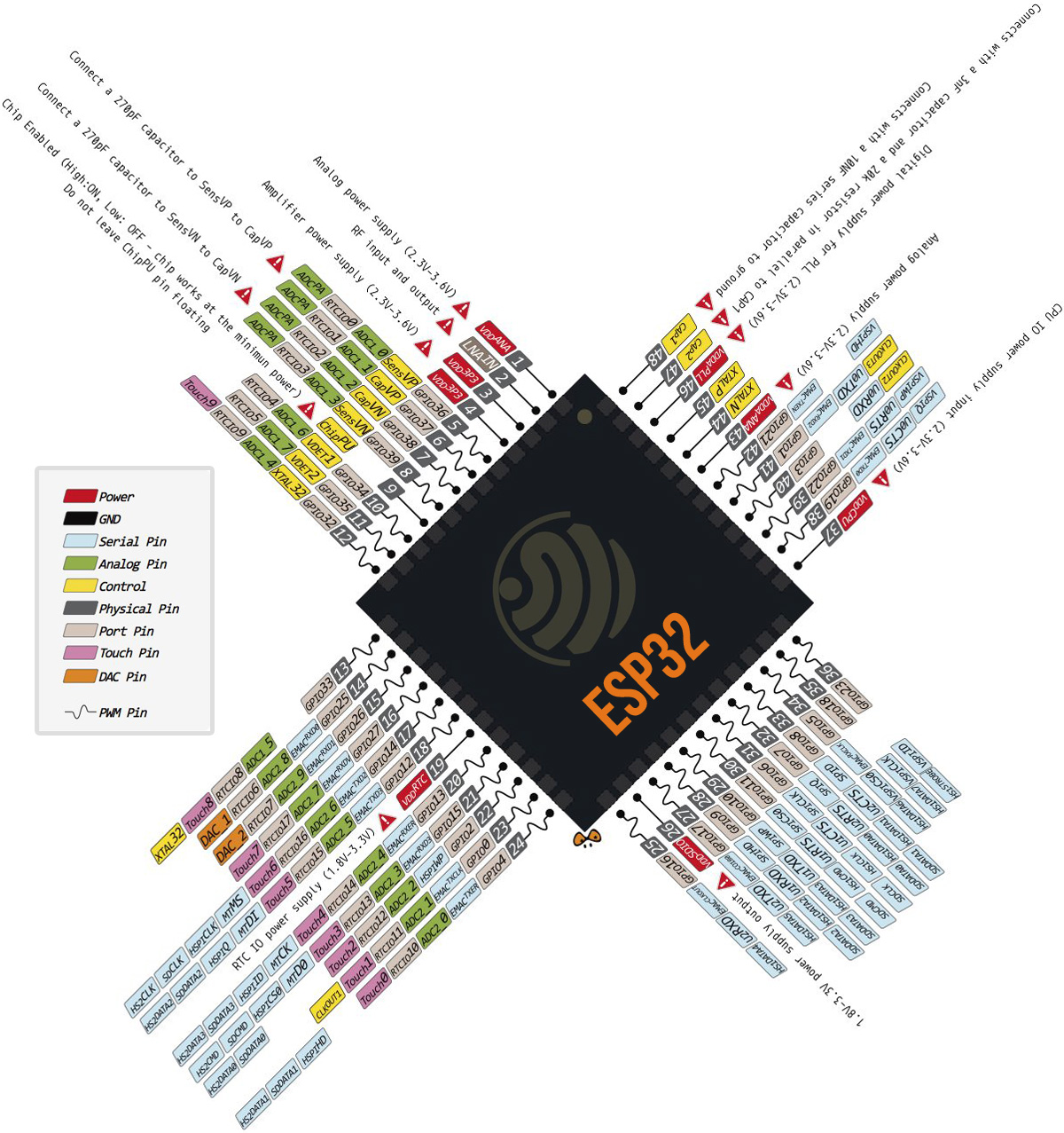
ESP32 Microcontroller Pinout Configuration
|
Pin Number |
Pin Name |
Description |
|
1 |
VDDA |
Analog power supply (2.3 V ∼ 3.6 V) |
|
2 |
LNA_IN |
RF input and output |
|
3 |
VDD3P3 |
Analog power supply (2.3 V ∼ 3.6 V) |
|
4 |
VDD3P3 |
Analog power supply (2.3 V ∼ 3.6 V) |
|
5 |
SENSOR_VP |
GPIO36, ADC1_CH0, RTC_GPIO0 |
|
6 |
SENSOR_CAPP |
GPIO37, ADC1_CH1, RTC_GPIO1 |
|
7 |
SENSOR_CAPN |
GPIO38, ADC1_CH2, RTC_GPIO2 |
|
8 |
SENSOR_VN |
GPIO39, ADC1_CH3, RTC_GPIO3 |
|
9 |
CHIP_PU |
High: On; enables the chip Low: Off; the chip powers off Note: Do not leave the CHIP_PU pin floating. |
|
10 |
VDET_1 |
GPIO34, ADC1_CH6, RTC_GPIO4 |
|
11 |
VDET_2 |
GPIO35, ADC1_CH7, RTC_GPIO5 |
|
12 |
32K_XP |
GPIO32, ADC1_CH4, RTC_GPIO9, TOUCH9, 32K_XP (32.768 kHz crystal oscillator input) |
|
13 |
32K_XN |
GPIO33, ADC1_CH5, RTC_GPIO8, TOUCH8, 32K_XN (32.768 kHz crystal oscillator output) |
|
14 |
GPIO25 |
GPIO25, ADC2_CH8, RTC_GPIO6, DAC_1, EMAC_RXD0 |
|
15 |
GPIO26 |
GPIO26, ADC2_CH9, RTC_GPIO7, DAC_2, EMAC_RXD1 |
|
16 |
GPIO27 |
GPIO27, ADC2_CH7, RTC_GPIO17, TOUCH7, EMAC_RX_DV |
|
17 |
MTMS |
GPIO14, ADC2_CH6, RTC_GPIO16, TOUCH6, EMAC_TXD2, HSPICLK, HS2_CLK, SD_CLK, MTMS |
|
18 |
MTDI |
GPIO12, ADC2_CH5, RTC_GPIO15, TOUCH5, EMAC_TXD3, HSPIQ, HS2_DATA2, SD_DATA2, MTDI |
|
19 |
VDD3P3_RTC |
Input power supply for RTC IO (2.3 V ∼ 3.6 V) |
|
20 |
MTCK |
GPIO13, ADC2_CH4, RTC_GPIO14, TOUCH4, EMAC_RX_ER, HSPID, HS2_DATA3, SD_DATA3, MTCK |
|
21 |
MTDO |
GPIO15, ADC2_CH3, RTC_GPIO13, TOUCH3, EMAC_RXD3, HSPICS0, HS2_CMD, SD_CMD, MTDO |
|
22 |
GPIO2 |
GPIO2, ADC2_CH2, RTC_GPIO12, TOUCH2, HSPIWP, HS2_DATA0, SD_DATA0 |
|
23 |
GPIO0 |
GPIO0, ADC2_CH1, RTC_GPIO11, TOUCH1, EMAC_TX_CLK, CLK_OUT1, |
|
24 |
GPIO4 |
GPIO4, ADC2_CH0, RTC_GPIO10, TOUCH0, EMAC_TX_ER, HSPIHD, HS2_DATA1, SD_DATA1 |
|
25 |
GPIO16 |
GPIO16, HS1_DATA4, U2RXD, EMAC_CLK_OUT |
|
26 |
VDD_SDIO |
Output power supply: 1.8 V or the same voltage as VDD3P3_RTC |
|
27 |
GPIO17 |
GPIO17, HS1_DATA5, U2TXD, EMAC_CLK_OUT_180 |
|
28 |
SD_DATA_2 |
GPIO9, HS1_DATA2, U1RXD, SD_DATA2, SPIHD |
|
29 |
SD_DATA_3 |
GPIO10, HS1_DATA3, U1TXD, SD_DATA3, SPIWP |
|
30 |
SD_CMD |
GPIO11, HS1_CMD, U1RTS, SD_CMD, SPICS0 |
|
31 |
SD_CLK |
GPIO6, HS1_CLK, U1CTS, SD_CLK, SPICLK |
|
32 |
SD_DATA_0 |
GPIO7, HS1_DATA0, U2RTS, SD_DATA0, SPIQ |
|
33 |
SD_DATA_1 |
GPIO8, HS1_DATA1, U2CTS, SD_DATA1, SPID |
|
34 |
GPIO5 |
GPIO5, HS1_DATA6, VSPICS0, EMAC_RX_CLK |
|
35 |
GPIO18 |
GPIO18, HS1_DATA7, VSPICLK |
|
36 |
GPIO23 |
GPIO23, HS1_STROBE, VSPID |
|
37 |
VDD3P3_CPU |
Input power supply for CPU IO (1.8 V ∼ 3.6 V) |
|
38 |
GPIO19 |
GPIO19, U0CTS, VSPIQ, EMAC_TXD0 |
|
39 |
GPIO22 |
GPIO22, U0RTS, VSPIWP, EMAC_TXD1 |
|
40 |
U0RXD |
GPIO3, U0RXD, CLK_OUT2 |
|
41 |
U0RXD |
GPIO1, U0TXD, CLK_OUT3, EMAC_RXD2 |
|
42 |
GPIO21 |
GPIO21, VSPIHD, EMAC_TX_EN |
|
43 |
VDDA |
Analog power supply (2.3 V ∼ 3.6 V) |
|
44 |
XTAL_N |
External crystal output |
|
45 |
XTAL_P |
External crystal input |
|
46 |
VDDA |
Analog power supply (2.3 V ∼ 3.6 V) |
|
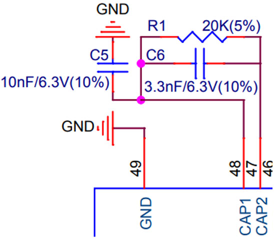
47 |
CAP2 |
Connects to a 3.3 nF (10%) capacitor and 20 k Ω resistor in parallel to CAP1 |
|
48 |
CAP1 |
Connects to a 10 nF series capacitor to ground |
|
49 |
GND |
Ground |
Features & Specifications
- 802.11 b/g/n where 802.11 n (2.4 GHz), up to 150 Mbps
- WMM
- TX/RX A-MPDU, RX A-MSDU
- Immediate Block ACK
- Defragmentation
- Automatic Beacon monitoring (hardware TSF)
- 4 × virtual Wi-Fi interfaces
- Simultaneous support for Infrastructure Station, SoftAP, and Promiscuous modes
- Antenna diversity
- Compliant with Bluetooth v4.2 BR/EDR and BLE specifications
- Class-1, class-2, and class-3 transmitter without external power amplifier
- Enhanced Power Control
- +12 dBm transmitting power
- NZIF receiver with –94 dBm BLE sensitivity
- Adaptive Frequency Hopping (AFH)
- Standard HCI based on SDIO/SPI/UART
- High-speed UART HCI, up to 4 Mbps
- Bluetooth 4.2 BR/EDR BLE dual-mode controller
- Synchronous Connection-Oriented/Extended (SCO/eSCO)
- CVSD and SBC for audio codec
- Bluetooth Piconet and Scatternet
- Multi-connections in Classic BT and BLE
- Simultaneous advertising and scanning
- Xtensa® single-/dual-core 32-bit LX6 microprocessor(s), up to 600 MIPS
- 448 KB ROM
- 520 KB SRAM
- 16 KB SRAM in RTC
- QSPI supports multiple flash/SRAM chips
Note: Complete technical details can be found in the ESP32 datasheet given at the end of this page.
Where to use ESP32 Wi-Fi & Bluetooth MCU
The ESP32 is designed for low-power IoT applications. Its high processing power with in-built Wi-Fi / Bluetooth and Deep Sleep Operating capabilities makes it ideal for most Portable IoT devices. Also, since Arduino IDE has officially released board managers for ESP32, it has become very easy to program these devices. A basic function diagram of the ESP32 Wi-Fi chip is shown below.
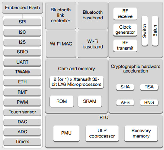
This has many features including, SPI, I2C, I2S, UART, ETH, RMT, PWM, ADC, DAC, Timers, Bluetooth, Wi-Fi RTC, and more, so with these features in made this device can do many things.
How to use ESP32 Wi-Fi & Bluetooth MCU
If you are designing your own product with this IC this can be on the complicated side of things because there is a ton of multiplexed IO that changes its characteristics when you try to enable or disable a feature, it's highly recommended to take a look at the datasheet for a certain application, you can also check out the hardware design guide for the ESP32 IC, the example below gives you a basic idea about how to properly configure this IC for a proper operation.
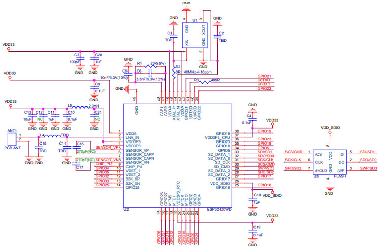
The handwear design of the ESP32 can be broken down into ten different parts, Power Supply, Power on Sequence and system Reset, Flash and PSRAM, Crystal Oscillator, RF, ADC, External Capacitors, UART, UART, SDIO, Touch Sensor.
Power Supply
VDD_SDIO connects to the output of an internal LDO, whose input is VDD3P3_RTC. When VDD_SDIO is connected to the same PCB net together with VDD3P3_RTC; the internal LDO is disabled automatically. The internal LDO can be configured as 1.8V, or the same voltage as VDD3P3_RTC. It can be powered off via software to minimize the current of Flash/SRAM during the Deep-sleep mode.
Digital Power Supply
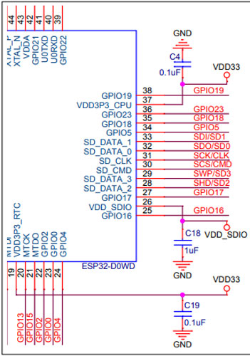
Pin19 and pin37 are the power supply pins for RTC and CPU, respectively. The digital power supply operates in a voltage range of 1.8 V ~ 3.6 V. We recommend adding extra filter capacitors of 0.1 µF close to the digital power supply pins.
Pin19 and pin37 are the power supply pins for RTC and CPU, respectively. The digital power supply operates in a voltage range of 1.8 V ~ 3.6 V. We recommend adding extra filter capacitors of 0.1 µF close to the digital power supply pins.
VDD_SDIO (pin26) works as the power supply for the related IO, and also for an external device.
- When VDD_SDIO operates at 1.8 V, it can be generated from ESP32’s internal LDO. The maximum current this LDO can offer is 40 mA, and the output voltage range is 1.65 V ~ 2.0 V. When the VDD_SDIO outputs 1.8 V, the value of GPIO12 should be set to 1 when the chip boots and it is recommended that users add a 2 kΩ ground resistor and a 4.7 µF filter capacitor close to VDD_SDIO
- When VDD_SDIO operates at 3.3 V, it is driven directly by VDD3P3_RTC through a 6 Ω resistor, therefore, there will be some voltage drop from VDD3P3_RTC. When the VDD_SDIO outputs 3.3 V, the value of GPIO12 is 0 (default) when the chip boots, and it is recommended that users add a 1 µF capacitor close to VDD_SDIO
VDD_SDIO can also be driven by an external power supply. The schematic for ESP32 digital power supply pins is shown in Figure
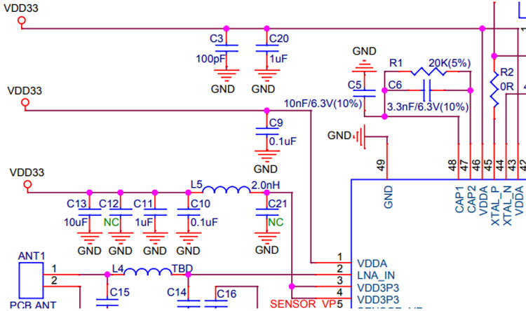
Analog Power Supply
Pin1, pin3, pin4, pin43, and pin46 are the analogy power supply pins. It should be noted that the sudden increase in the current draw, when ESP32 is in transmission mode, may cause a power rail collapse. Therefore, it is highly recommended to add another 10 µF capacitor to the power trace, which can work in conjunction with the 0.1 µF capacitor. LC filter circuit needs to be added near the power pin so as to suppress high-frequency harmonics. The inductor’s rated current is preferably 500 mA and above.
Power-on Sequence and system Reset
ESP32 uses a 3.3 V system power supply. The chip should be activated after the power rails have stabilized. This is achieved by delaying the activation of CHIP_PU (Pin9) after the 3.3 V rails have been brought up. More details can be found in Section Power Scheme.
To avoid reboots caused by external interferences, the CHIP_PU trace should be as short as possible and routed away from the clock lines. A pull-up resistor and a ground capacitor are highly recommended.
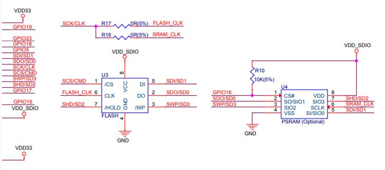
Flash and PSRAM
ESP32 can support up to 16 MB external flash and 8 MB external SRAM. The example module described in this document uses a 4 MB flash by default. The VDD_SDIO acts as the power supply pin. Make sure to select the appropriate flash according to the power voltage on VDD_SDIO. On PSRAM, all pins except for the CS pin can be multiplexed with flash. For example, PSRAM_CLK and FLASH_CLK share the same SCK/CLK pin of ESP32 to use the pins efficiently, but in some ESP32 modules, such as ESP32-WROVER-E, flash has its own clock pin: SCK/CLK, and PSRAM uses GPIO17. The schematic of connections of ESP32 with flash and PSRAM is shown in Figure 4. Note that the connection shown in Figure 4 is not the only way to connect flash and PSRAM.
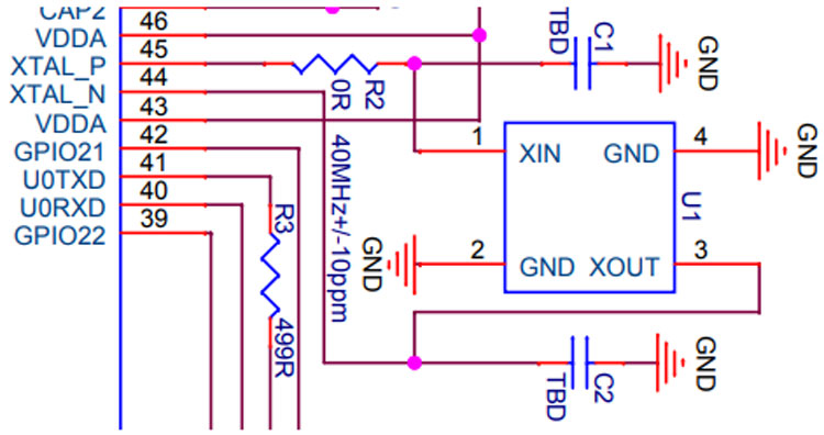
External Clock Source and RTC Clock Source
Currently, the ESP32 Wi-Fi/BT firmware only supports a 40 MHz crystal oscillator. In circuit design, capacitors C1 and C2 which connect to the ground are added to the input and output terminals of the crystal oscillator respectively. It is recommended that users reserve a series resistor of 0 Ω on the XTAL_P clock trace to reduce the drive strength of the crystal, as well as to minimize the impact of crystal harmonics on RF performance.
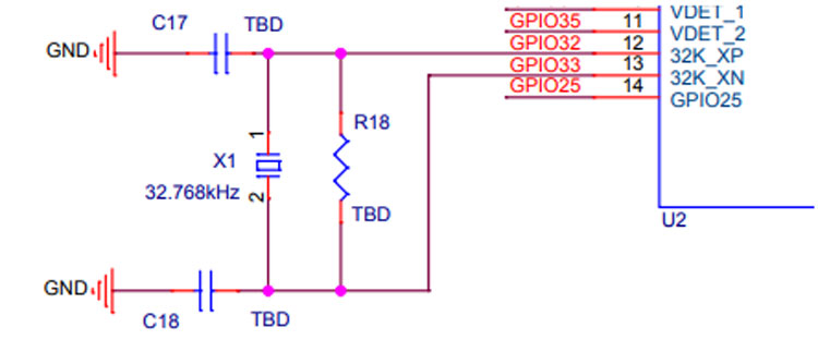
ESP32 supports an external 32.768 kHz crystal or an external 32.768 kHz signal (e.g., an oscillator) to act as the RTC sleep clock.
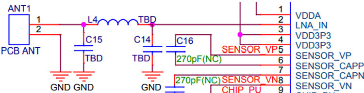
RF Output
The output impedance of the RF pins of ESP32 (QFN 6*6) and ESP32 (QFN 5*5) is (30+j10) Ω and (35+j10) Ω, respectively. A π-type matching network is essential for antenna matching in the circuit design. CLC structure is recommended for the matching network. The schematic for ESP32 RF circuitry is shown in the figure below:
External Capacitor
shows the schematic of components connected to pin47 CAP2 and pin48 CAP1. C5 (10 nF) that connects to CAP1 should be of 10% tolerance and is required for proper operation of ESP32. RC circuits between CAP1 and CAP2 pins may be omitted under certain conditions. This circuit is used when entering Deep-sleep mode. During this process, to minimize power consumption, the voltage to power ESP32 internals is dropped from 1.1 V to around 0.7 V. The RC circuit is used to minimize the period of the voltage drop. If removed, this process will take longer and the power consumption in Deep-sleep will be higher. If a particular application of ESP32 is not using Deep-sleep mode, or power consumption is less critical, then this circuit is not required.
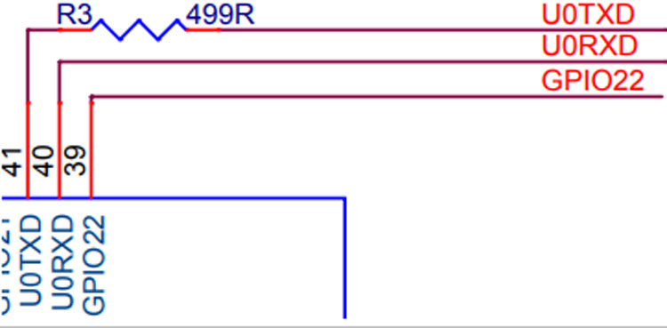
UART
Users need to connect a 499 Ω resistor to the U0TXD line in order to suppress the 80 MHz harmonics. The schematic for ESP32 UART is shown in Figure:
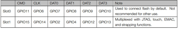
SDIO
There are two sets of GPIOs (slot0 and slot1) that can be assigned to SDIO on ESP32, as shown in the table below. When ESP32 works as an SDIO host or slave, connect GPIOs in slot1 to signal lines
Touch Sensor
When using the touch function, it is recommended to reserve a series resistor at the chip side to reduce the coupling noise and interference on the line and to strengthen the ESD protection. The recommended resistance is 470 Ω ~ 2 kΩ, preferably 510 Ω. The specific value also depends on the testing of the product
Applications
- Generic Low-power IoT Sensor Hub
- Generic Low-power IoT Data Loggers
- Cameras for Video Streaming
- Over-the-top (OTT) Devices
- Speech Recognition
- Image Recognition
- Mesh Network
- Home Automation: Light control, Smart Plug, Smart Door Lock
- Smart Building: Smart Light, Energy Monitor
- Industrial Automation: Industrial Wireless Control, Industrial Robotics
- Smart Agriculture: Smart Greenhouses, Smart Irrigation, Agriculture Robotics
- Audio Applications: Internet Music Players, Live Stream Device, Audio Headset
- Health Care Applications: Health Monitor, Baby Monitor
- Wearable Electronics: Smart Watches, Smart Bracelets
- Retail & Catering Applications: POS Machine, Service Robotics
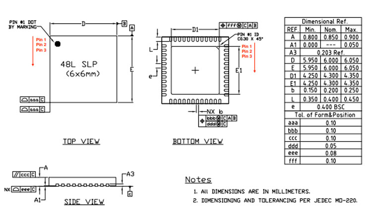
2D Model and Dimensions
If you are designing a PCB or Perf board with this component then the following picture from the Datasheet will be useful to know its package type and dimensions.