TIP42C PNP Power Transistor Pinout, Specifications, Equivalent & Datasheet
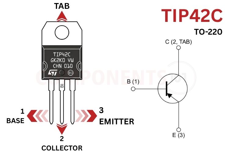
TIP42C Pinout Configuration
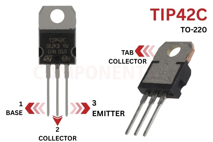
The TIP42C is a PNP silicon power transistor rated for -100V collector-emitter voltage, -6A continuous collector current and 65W power dissipation, in a 3-pin TO-220 package. The TIP42C pinout follows the standard TO-220 layout.
| Pin Number | Pin Name | Description |
| 1 | Base (B) | Controls the PNP transistor's conduction state. Sinking current out of the base turns the transistor ON. |
| 2 | Collector (C) | High-current collector terminal connected to the load and internally bonded to the metallic heatsink tab. |
| 3 | Emitter (E) | Power terminal connected to the positive DC power supply rail in typical high-side switching circuits. |
| Tab | Collector (C) | Metallic mounting tab electrically connected to Pin 2 Collector for efficient thermal dissipation. |
TIP42 Series Voltage Grades: TIP42 vs TIP42A vs TIP42B vs TIP42C
The TIP42 transistor series is produced in four breakdown voltage ratings. The letter suffix printed on the TO-220 package designates the maximum collector-emitter voltage threshold:
| Model Variant | Collector-Emitter Voltage (VCEO) | Collector-Base Voltage (VCBO) | Continuous Collector Current (IC) | Typical Voltage Suitability |
| TIP42 | -40V | -40V | -6A | Low-voltage 12V automotive and consumer portable electronics. |
| TIP42A | -60V | -60V | -6A | 24V industrial controls, solenoid drivers, and audio amplifiers. |
| TIP42B | -80V | -80V | -6A | 36V to 48V telecom equipment and medium-power audio systems. |
| TIP42C | -100V | -100V | -6A | Premium high-voltage variant; universally replaces TIP42, TIP42A, and TIP42B |
*Note: Because the TIP42C provides the highest -100V breakdown margin at the same price point and physical footprint, engineers and repair technicians universally standardise the TIP42C as a universal replacement across all lower-voltage TIP42 variants.
TIP42C Key Features & Specifications
- Transistor Polarity / Type: PNP Epitaxial-Base Silicon Power Transistor
- Collector-Emitter Voltage (VCEO): -100V (IB = 0)
- Collector-Base Voltage (VCBO): -100V (IE = 0)
- Emitter-Base Voltage (VEBO): -5.0V (IC = 0)
- Continuous Collector Current (IC): -6.0 A
- Peak Pulsed Collector Current (ICM): -10.0 A
- Continuous Base Current (IB): -2.0A (STMicroelectronics models rated up to -3.0A)
- Total Power Dissipation (PD): 65W at TC = 25°C (2.0W at ambient TA = 25°C in free air)
- Collector-Emitter Saturation Voltage (VCE(sat)): -1.5V max at IC = -6.0A, IB = -600 mA
- Base-Emitter On Voltage (VBE(on)): -2.0V max at VCE = -4.0V, IC = -6.0A
- DC Current Gain (hFE): 30 min (at VCE = -4V, IC = -0.3A); 15 to 75 (at VCE = -4V, IC = -3.0A)
- Transition Frequency (fT): 3.0 MHz min at VCE = -10V, IC = -0.5A, f = 1.0 MHz
- Operating Junction Temperature (Tj): -65°C to +150°C
- Thermal Resistance (RthJC): 1.92 °C/W (Junction-to-Case)
- Package Type: TO-220 (TO-220AB / 3-Pin Through-Hole)
*Note: Complete Technical Details can be found in the TIP42C datasheet given at the end of this page.
TIP42C Datasheet
The complete original manufacturer technical specifications, safe operating area (SOA) curves, and saturation voltage performance plots are available in the official PDF TIP42C datasheet.
TIP42C Equivalent and Alternative Transistors
A suitable TIP42C equivalent must be PNP, share the same pinout and meet or exceed the voltage, current and power requirements of your circuit.
| Equivalent Part | Polarity | Key Ratings | Description & Compatibility Notes |
| TIP41C | NPN | 100V, 6A, 65W, TO-220 | Exact complementary NPN partner for push-pull audio amplifier output stages. |
| BD244C | PNP | -100V, -6A, 65W, TO-220 | European standard direct drop-in replacement with matching pinout and specifications. |
| TIP32C | PNP | -100V, -3A, 40W, TO-220 | Lower-current (3A) sibling; suitable for lighter loads up to 2A. |
| MJE2955T | PNP | -60V, -10A, 75W, TO-220 | Higher-current TO-220 PNP power transistor for circuits operating below 60V. |
| 2N6491 | PNP | -80V, -15A, 75W, TO-220 | High-current alternative for heavy-duty DC switching and audio power stages. |
| TIP127 | PNP | -100V, -5A, Darlington, TO-220 | High-gain Darlington PNP alternative (hFE > 1000) for direct low-current microcontroller control. |
What Is the TIP42C Transistor?
The TIP42C is an iconic discrete power semiconductor in modern power electronics. As a PNP bipolar junction transistor, its conduction mechanism operates opposite to an NPN device: current enters the Emitter (Pin 3) and exits through the Collector (Pin 2). Conduction is initiated when the Base (Pin 1) voltage is pulled at least 0.7V lower than the Emitter voltage, allowing current to be drawn out of the base terminal.
Key operational characteristics of the TIP42C include:
1. High-Side Power Switching Advantage: Unlike NPN transistors or N-channel MOSFETs that require complex bootstrap charge pumps or floating gate drivers to switch loads on the positive supply rail, the TIP42C connects its Emitter directly to the positive DC bus (+12V or +24V). This allows simple, referenced high-side switching where the load remains permanently grounded.
2. Complementary Push-Pull Symmetry: In Class AB audio amplifiers, symmetrical reproduction of the negative audio waveform requires a PNP power transistor whose transfer characteristics, frequency response, and current handling precisely match the high-side NPN device. The TIP42C is specifically processed to mirror the electrical curves of the TIP41C.
3. Saturation Base Current Requirements: At high collector currents (such as IC = 3A to 6A), the current gain (hFE) of the TIP42C drops into the 15 to 30 range. To ensure complete saturation and minimize collector-emitter dissipation, circuit designers must size the base driver to extract between 150 mA and 300 mA of base current (IB ≥ IC / 15).
4. Heatsinking and Tab Isolation: The metallic mounting tab of the TO-220 package is internally bonded to Pin 2 Collector. In high-side switching circuits where the collector is wired to the load, the heatsink tab will toggle between ground and +VCC. If mounting to a shared metal chassis, an insulating mica or sil-pad kit with a nylon shoulder washer must be used to prevent short circuits.
TIP42C Circuit Diagram: High-Side Load Switch
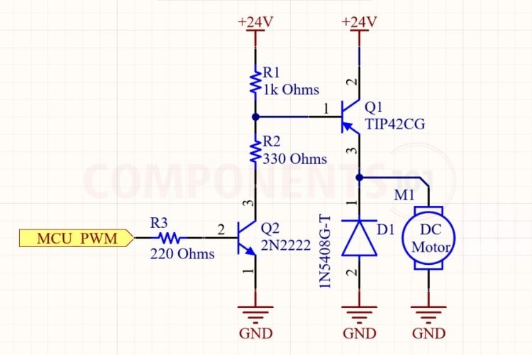
A prominent practical implementation of the TIP42C circuit diagram is a High-Side DC Load Switch driven by the low-voltage 3.3V or 5V GPIO pin of a microcontroller (such as an Arduino, ESP32, or STM32).
Circuit Operation & Component Selection
1. Pull-Up Resistor (R1 = 1 kΩ):
Because the TIP42C Emitter is tied directly to the +12V or +24V power rail, its Base must sit at the same positive voltage when turned OFF. Resistor R1 pulls the Base up to +VCC, ensuring VBE = 0V and keeping the TIP42C firmly in cutoff when no drive signal is present.
2. NPN Level-Shifter Transistor (Q2 = 2N2222A or BC547):
A microcontroller GPIO cannot be connected directly to the base of a high-side PNP transistor because its maximum pin voltage (3.3V or 5V) is far below the +12V rail, which would leave the PNP permanently turned ON. Small-signal NPN transistor Q2 acts as an open-collector level shifter:
When the MCU output is LOW (0V), Q2 is OFF. Resistor R1 holds the TIP42C Base at +12V, and the load remains unpowered.
When the MCU output is HIGH (5V), Q2 saturates, pulling current down through base resistor R2 to ground. This sinks current out of the TIP42C Base, causing the PNP to switch fully ON and deliver power to the load.
3. Base Limiting Resistor (R2 = 330 Ω, 0.5W):
Resistor R2 sets the saturation base current extracted from the TIP42C. With a 12V rail, a TIP42C VBE drop of 0.8V, and a Q2 saturation drop of 0.2V, the base current is:
IB = (12 V - 0.8V - 0.2V) / 330 Ω ≈ 33 mA.
This provides sufficient base drive to saturate the TIP42C for loads drawing up to 1.0A to 1.5A. For maximum 6A loads, R2 can be decreased to 100 Ω (1W) to supply roughly 110 mA of base drive.
4. Inductive Flyback Clamping Diode (1N5408 / 1N5822):
When driving inductive loads (such as DC motors, solenoids, or magnetic relays), an inductive voltage spike of opposite polarity is induced when the TIP42C switches OFF. A 3A fast-recovery diode (such as a 1N5408) connected across the load terminals clamps this back-EMF spike safely to ground, shielding the TIP42C collector from exceeding its -100V breakdown threshold.
Applications of the TIP42C Transistor
- Class AB Audio Amplifiers: Power output push-pull pairs in Hi-Fi stereo power amplifiers, instrument amplifiers, active monitors, and intercoms (paired with TIP41C).
- High-Side Load Switching: High-current switching for grounded industrial actuators, solenoids, and automotive accessories.
- Linear DC Voltage Regulators: Series-pass elements in low-dropout (LDO) and dual-rail positive/negative bench power supplies.
- H-Bridge Motor Drives: High-side switching stages in bidirectional DC motor H-bridge driver circuits.
- Battery Disconnect & Reverse Polarity Protection: Power gating in battery management systems and emergency lighting backup circuits.
- Relay & Contactor Actuation: High-current driver stages for industrial automation contactors and automotive lighting relays.
TIP42C 2D Model and Package Dimensions
For PCB layout engineers creating footprints in EDA design tools (KiCad, Altium Designer, Eagle, EasyEDA), the physical dimensions for the standard TO-220 (TO-220AB) package are detailed below:
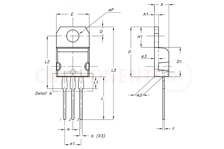
| Parameter Symbol & Description | Minimum (mm) | Typical (mm) | Maximum (mm) |
| A (Package Thickness / Total Depth) | 4.40 | 4.45 | 4.50 |
| A1 (Heatsink Tab Thickness) | 1.22 | - | 1.32 |
| A2 (Base to Seating Plane) | 2.49 | 2.59 | 2.69 |
| A3 (Step Thickness to Tab) | 1.17 | 1.27 | 1.37 |
| b (Lead Width, X3) | 0.78 | - | 0.87 |
| c (Lead Thickness) | 0.49 | - | 0.56 |
| D (Total Body Length / Height) | 15.40 | 15.50 | 15.60 |
| D1 (Lower Moulded Body Height) | 9.05 | 9.15 | 9.25 |
| E (Total Body Width) | 10.08 | 10.18 | 10.28 |
| e (Lead Pitch / Pin Spacing) | 2.44 | 2.54 | 2.64 |
| e1 (Total Pin 1 to Pin 3 Spacing) | 4.98 | 5.08 | 5.18 |
| H1 (Heatsink Tab Height) | 6.25 | 6.35 | 6.45 |
| L (Lead Length from Body) | 13.20 | 13.40 | 13.60 |
| L1 (Lead Shoulder Length) | 3.50 | 3.70 | 3.90 |
| L2 (Hole Center to Lead Shoulder) | 16.30 | 16.40 | 16.50 |
| L3 (Overall Package Length with Leads) | 28.70 | 28.90 | 29.10 |
| ØP (Mounting Hole Diameter) | 3.75 | 3.80 | 3.85 |
| Q (Tab Top to Hole Center) | 2.70 | 2.80 | 2.90 |