AO3400A N-Channel MOSFET Pinout, Specifications, Marking Code & Datasheet
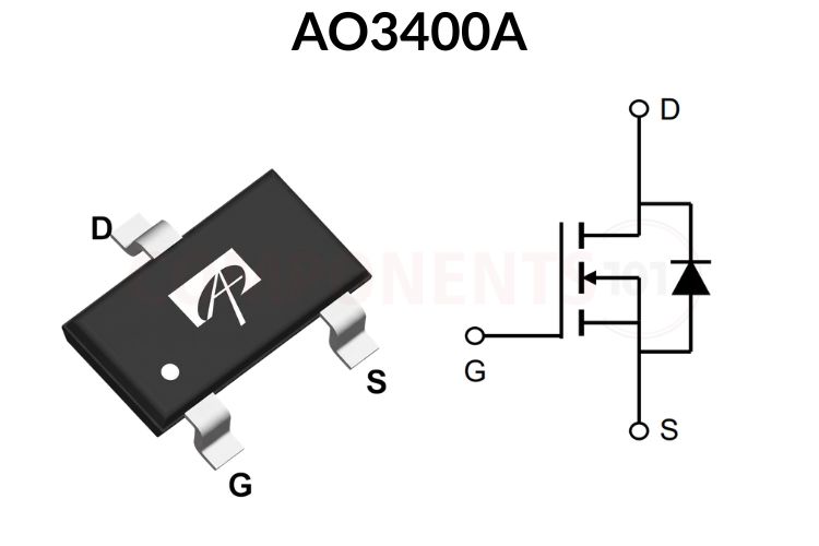
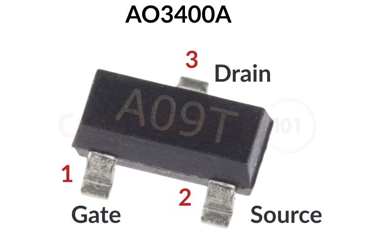
AO3400A Pinout Diagram & Pin Configuration
| Pin Number | Pin Name | Description |
| 1 | Gate (G) | Controls the biasing and switching of the MOSFET. Applying a positive voltage relative to the source turns the channel ON. |
| 2 | Source (S) | Current drains out through the source terminal. Typically tied to system ground in low-side switching configurations. |
| 3 | Drain (D) | Current flows into the MOSFET through the drain terminal. Connected to the negative terminal of the load. |
AO3400A SMD Marking Code (A09T MOSFET Identification)
Because SOT-23 packages are extremely small (2.9 mm × 1.3 mm), manufacturers print shorthand SMD marking codes rather than the full part number:
| Marking Code | Manufacturer / Variant | Package | Notes |
| A09T | Alpha & Omega Semiconductor (AOS) | SOT-23 | Most common official marking code worldwide. |
| X0DV | Alternate / OEM Variant | SOT-23 | Common marking code found on JLCPCB / LCSC basic stock. |
| 3400 | Second-source Clone | SOT-23 | Generic Chinese second-source fab marking. |
*Note: Suffix characters or vertical bars next to the marking code indicate the production year, week, or fab lot trace code.
AO3400A Datasheet: Key Specifications & Ratings
- Transistor Polarity: N-Channel Enhancement Mode
- Drain-Source Voltage (VDS): 30V
- Continuous Drain Current (ID): 5.7A (@ VGS = 10V, TA = 25°C); 4.7A (@ TA = 70°C)
- Pulsed Drain Current (IDM): 30A
- Gate-Source Voltage (VGS): ±12V
- Low On-State Resistance (RDS(on)): < 26.5 mΩ @ VGS = 10V; < 32 mΩ @ VGS = 4.5V; < 48 mΩ @ VGS = 2.5V
- Gate Threshold Voltage (VGS(th)): 0.65V (Min) to 1.45V (Max) (Fully compatible with 2.5V, 3.3V, and 5V logic)
- Total Gate Charge (Qg): 6 nC (Typ @ 4.5V)
- Maximum Power Dissipation (PD): 1.4W (TA = 25°C)
- Operating Junction & Storage Temperature: -55°C to +150°C
- Package Type: SOT-23-3L (Surface Mount)
*Note: Complete Technical Details can be found in the AO3400A datasheet given at the end of this page.
AO3400A Equivalent & Alternative MOSFETs
| Equivalent Part | Polarity | Key Ratings | Description / Notes |
| AO3401A | P-Channel | -30V / -4.0A / 44 mΩ | Direct complementary P-Channel pair. Ideal for high-side switching and reverse battery polarity protection. |
| SI2302 / SI2302CDS | N-Channel | 20V / 2.8A / 55 mΩ | Widely available low-voltage SMD N-channel MOSFET in SOT-23. |
| IRLML2502 | N-Channel | 20V / 4.2A / 45 mΩ | International Rectifier logic-level miniature MOSFET (Micro3 / SOT-23). |
| DMG3420U | N-Channel | 20V / 5.7A / 26 mΩ | High-current logic-level substitute from Diodes Inc. (SOT-23). |
| 2N7002 | N-Channel | 60V / 115mA / 5 Ω | Low-current signal switching substitute only (cannot drive heavy loads). |
| IRLZ44N | N-Channel | 55V / 47A / 22 mΩ | Through-hole TO-220AB logic-level alternative for high-power prototyping. |
Brief Description of AO3400A
The AO3400A is widely considered the industry-standard SMD N-channel MOSFET in consumer gadgets, IoT modules, and battery-operated hardware.
Standard power MOSFETs (like the IRF540N or IRFZ44N) require a gate-to-source voltage (VGS) of 10V to achieve full channel enhancement and minimal on-resistance. Driving them directly with a 3.3V microcontroller results in high channel resistance, massive heat dissipation, and severe voltage drops across the drain-to-source terminals.
In contrast, the AO3400A is optimised specifically as a sub-logic-level device. With a maximum gate threshold voltage (VGS(th)) of only 1.45V, the gate channel begins conducting well below 1.5V. At a 3.3V logic output, its internal resistance drops below 38 mΩ, allowing it to switch currents up to 3A - 4A continuously with negligible thermal rise and without heatsinking.
AO3400A Circuit Diagram: How to Use It with Arduino / ESP32
The AO3400A is typically deployed in a low-side switching configuration, where the MOSFET is positioned between the negative terminal of the load and system ground.
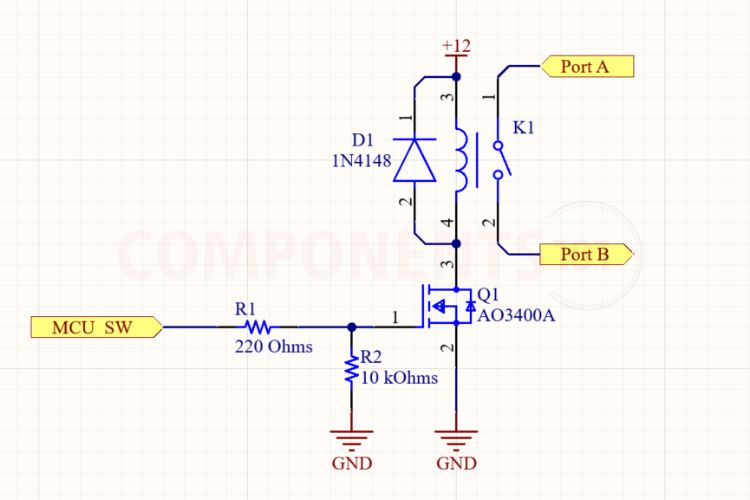
Circuit Operation & Component Selection
1. Gate Current-Limiting Resistor (RGATE):
Even though a MOSFET is a voltage-controlled device, its gate acts as a small capacitor (Ciss ≈ 630 pF). When an MCU GPIO pin switches HIGH, a momentary surge current rushes into the gate. Placing a 100 Ω to 220 Ω resistor in series between the MCU GPIO pin and the gate dampens parasitic ringing, protects the microcontroller GPIO output driver from inrush stress, and prevents high-frequency switching oscillations.
2. Gate Pull-Down Resistor (RGS):
During microcontroller power-on, reset, or bootloader execution, GPIO pins default to a high-impedance (floating) input state. Without a pull-down resistor, stray ambient capacitance or electrostatic charge can partially turn ON the MOSFET, inadvertently activating the load. A 10 kΩ pull-down resistor connected directly from Gate (Pin 1) to Source / GND (Pin 2) guarantees that the MOSFET remains solidly in the OFF (cutoff) state whenever the control signal is absent or floating.
3. Flyback Diode (D1 for Inductive Loads):
When switching inductive loads such as DC motors, solenoids, or relays, the collapsing magnetic field generates a severe high-voltage back-EMF spike that can exceed the AO3400A's 30V breakdown rating. Always place a fast diode (such as a 1N4148 for small relays or a 1N5819 / SS14 Schottky diode for DC motors) in reverse parallel across the inductive load terminals.
Applications
- Battery-Powered IoT Devices: Power gating and sleep-mode disconnect switches in ESP32, ESP8266, and nRF52 sensor nodes.
- Low-Side Load Switching: Controlling 5V/12V relays, solenoids, vibration motors, and buzzers from 3.3V microcontrollers.
- High-Efficiency PWM Dimming: LED strips, 12V cooling fans, and display backlights.
- DC Motor Control: Low-voltage H-bridges and unidirectional motor drivers for drones and robotics.
- Li-Ion Battery Protection Modules (BMS): Charge and discharge cut-off switches in 1S Lithium-Ion battery packs.
- Power Rail Sequencing: Clean switching between multiple supply rails in embedded hardware.
2D Model and Component Dimensions
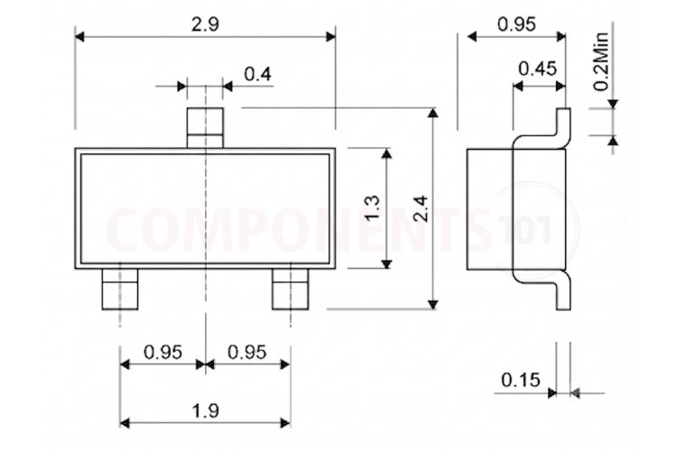
For engineers designing a custom PCB or adding the AO3400A footprint to CAD tools (KiCad, Altium, Eagle, EasyEDA), the physical dimensions for the standard SOT-23-3L package are given below:
| Dimension Parameter | Minimum (mm) | Typical (mm) | Maximum (mm) |
| Body Length (D) | 2.80 | 2.90 | 3.04 |
| Total Width (E) | 2.10 | 2.30 | 2.64 |
| Body Width (E1) | 1.20 | 1.30 | 1.40 |
| Total Height (A) | 0.89 | 1.00 | 1.14 |
| Lead Pitch (e) | - | 1.90 (typ) | - |
| Lead Width (b) | 0.30 | 0.40 | 0.50 |