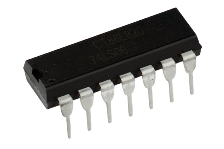
74LS06 Hex Inverter/Buffer IC
74LS06 NOT gate IC also called Hex Inverter, as it consists of 6 independent NOT gates. All of the inverter IC’s pins are TTL compatible, making it easy to use without any external circuitry. This IC can be used in multiple applications and can be used for signal generation, logic level converters, etc.
Features and Specifications
This section mentions some of the important features and specifications of the 74LS06 inverter.
- Supply voltage: 5V DC
- Maximum Input Voltage: 5.25V DC
- Output Current(HIGH): 0.4mA
- Output Current(LOW): 8.0mA
- Input HIGH-level voltage: 2V
- Input LOW-level voltage: 0.8V
- Output HIGH level Voltage(typical): 3.5V
- Output LOW level voltage(max): 0.5V
- Operating Temperature: 25 - 70 Degree C
Note: More technical information can be found in the 74LS06 datasheet, linked at the bottom of this page.
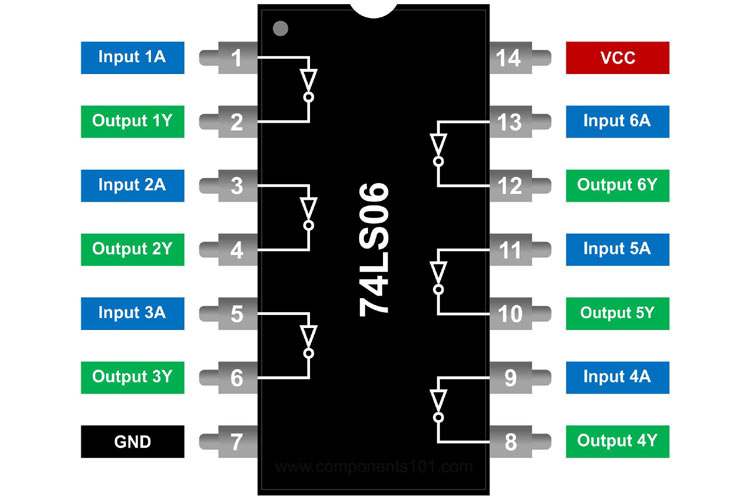
74LS06 IC Pinout Configuration
The Hex inverter IC has 6 NOT gates built-in. The IC has 14 pins, the table below depicts the pin configuration of the 74LS06 IC.
|
Pin Number |
Pin Type |
Pin Description |
|
1 |
Input 1A |
Input pin of NOT gate 1 |
|
2 |
Output 1Y |
Output pin of NOT gate 1 |
|
3 |
Input 2A |
Input pin of NOT gate 2 |
|
4 |
Output 2Y |
Output pin of NOT gate 2 |
|
5 |
Input 3A |
Input pin of NOT gate 3 |
|
6 |
Output 3Y |
Output pin of NOT gate 3 |
|
7 |
GND |
Ground |
|
8 |
Output 4Y |
Output pin of NOT gate 4 |
|
9 |
Input 4A |
Input pin of NOT gate 4 |
|
10 |
Output 5Y |
Output pin of NOT gate 5 |
|
11 |
Input 5A |
Input pin of NOT gate 5 |
|
12 |
Output 6Y |
Output pin of NOT gate 6 |
|
13 |
Input 6A |
Input pin of NOT gate 6 |
|
14 |
VCC |
Positive input voltage |
Internal Schematic and Boolean logic Table
74LS06 is an IC consisting of 6 independent NOT gates. It supports TTL signals, making it very easy to use. The IC’s internal schematic can be seen in the image below. Any input to Pin 1 gets inverted and the inverted output is received at Pin 2. This principle of inversion makes it ideal to use for multiple applications including signal wave generators, Buffer, etc.

The NOT gate IC(74LS06) has a simple boolean logic which can be understood by the truth table shown below.
|
Input(A) |
Output(Y) |
|
1 |
0 |
|
0 |
1 |
As mentioned in the features and specification section, the signal should have LOW-level input voltage as less or equal to 0.8V anything above it will be considered as a HIGH signal. The truth table shows the input side(A) and the output(Y), when a high signal(1) is provided to the input, we obtain a low signal(0) at the output terminal. Similarly, if a low signal(0) is provided at input a high signal(1) is observed at the output.
Here is a simulation of working of a NOT gate;

Alternatives
Available packages
PLASTIC PACKAGE CASE 646–06, PLASTIC SOIC PACKAGE CASE 751A–03
Applications
Here are some of the applications of the Inverter/NOT gate IC.
- Clock signal generators
- Buffer IC
- Logic Circuits
- Logic level converter
2D Model
Below is the 2D model of the 74LS06 along with its dimensions in millimeters and inches. The following information can be used while designing custom footprints of the IC and be used for PCB designing and CAD modellig.


