40V Low-Voltage Power MOSFET in PQFN Package with Greater Design Flexibility to Maximize System-Level Performance

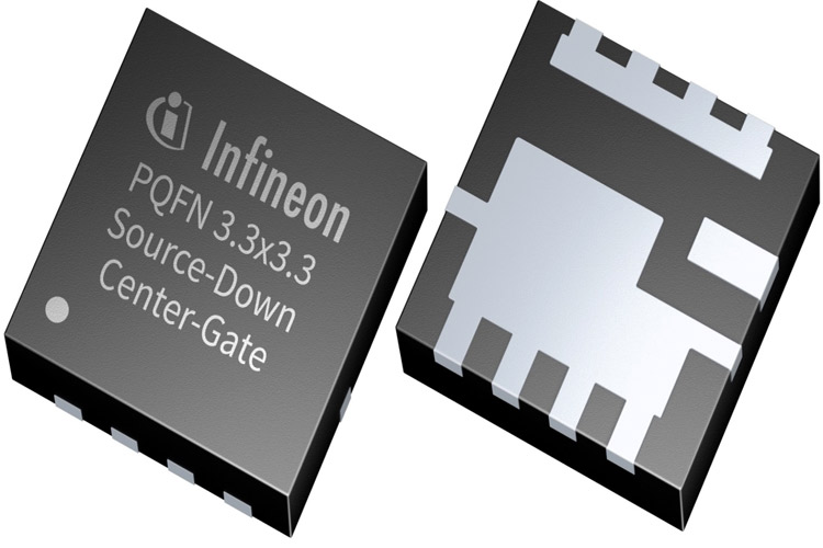
To provide high power density levels and small form factors to maximize system-level performance to the contemporary power system designs, Infineon Technologies has come up with the OptiMOS 40 V low-voltage power MOSFET packaged in the Source-Down (SD) PQFN with a 3.3 x 3.3 mm2 footprint. The 40 V SD MOSFET addresses SMPS for server, telecom, and OR-ing besides battery protection, power tool, and charger applications.
Compared to the current technology, this variant can lead to a major reduction of RDS(on) by up to 25 percent. The SD package features silicon, which is flipped upside down inside of the component, and the source potential is connected to the PCB over the thermal pad instead of the drain potential.
The SD OptiMOS can withstand high continuous currents of up to 194 A. Also, the thermal resistance between junctions to case (R thJC) is significantly better than the traditional PQFN packages up on the market shelves. Greater design flexibility enhanced performance is promised owing to optimized layout possibilities and efficient utilization of the PCB.
The OptiMOS SD 40 V low-voltage power MOSFET is available in two versions - Standard and Center-Gate (optimized for parallel operation of multiple devices). Both the variants in the PQFN 3.3 x 3.3 mm2 packages can be ordered from the company website.
Features of OptiMOS 40 V low-Voltage Power MOSFET
- Packaged in the Source-Down (SD) PQFN with a 3.3 x 3.3 mm2 footprint
- Ability to withstand high continuous currents of up to 194 A
- Major reduction of R DS(on) by up to 25 percent
Note: More technical information can be found in the OptiMOS 40 V low-voltage power MOSFET datasheet linked at the bottom of this page and on the OptiMOS 40 V low-voltage power MOSFET product page.


