Microchip’s 1.2V Clock Buffers Link Latest SoCs and FPGAs with Higher Voltage Components
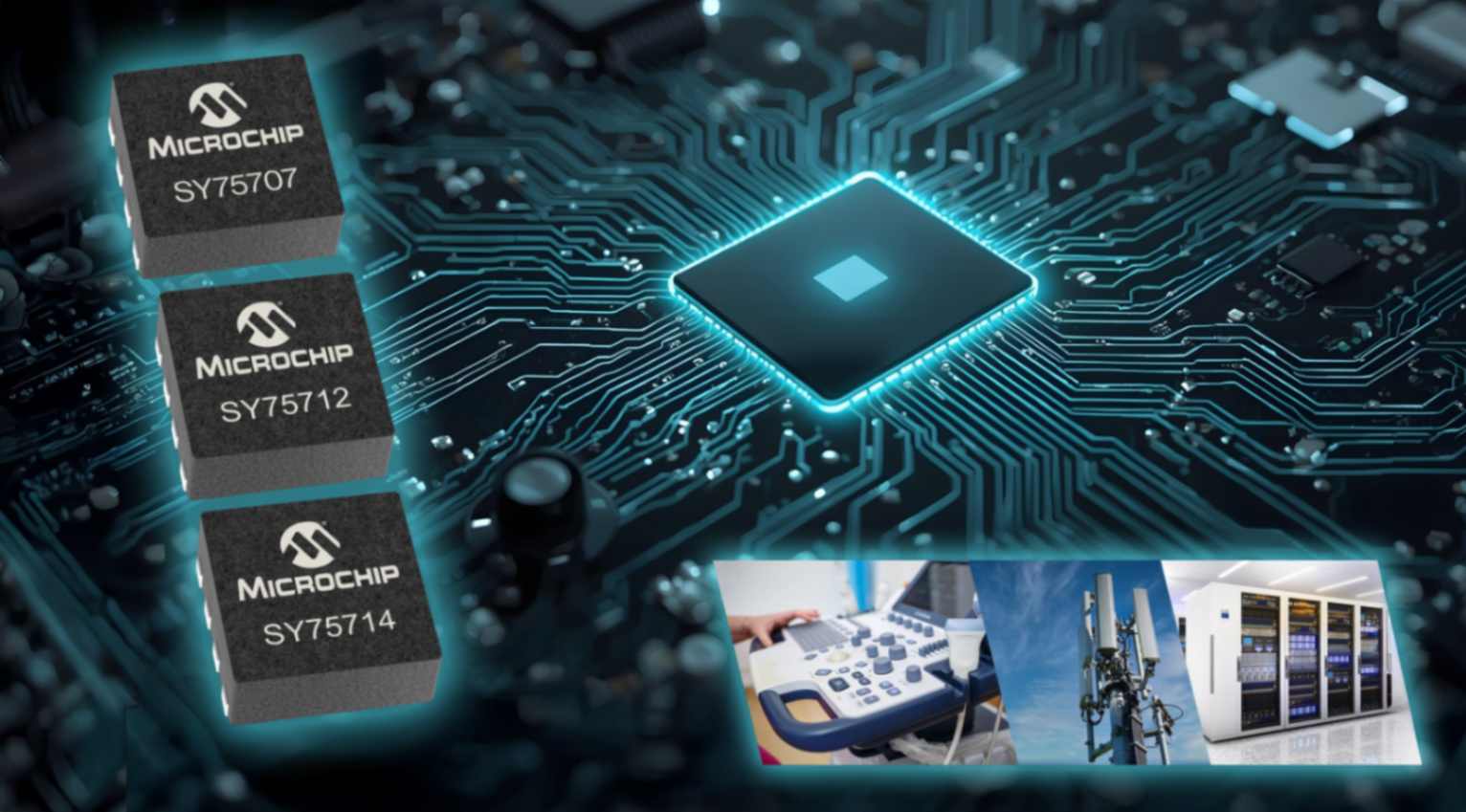
The rapid adoption of advanced FinFET process nodes in high-performance FPGAs, SoCs, AI accelerators, and next-generation CPUs has driven a growing demand for low-voltage clock drivers. Printed circuit board designers frequently encounter challenges due to the limited availability of standard 1.2V LVCMOS clock buffers and level-translating buffers capable of converting higher-voltage clock signals to the lower-voltage levels required by these advanced devices. Traditional approaches, relying on discrete components and voltage-divider techniques, can compromise signal integrity and clock duty-cycle accuracy, while also increasing board complexity and component count.
To address these critical design challenges, Microchip Technology has introduced the SY757xx family, a comprehensive portfolio of 1.2V-output LVCMOS clock buffers. These new devices simplify system design by eliminating the need for conventional discrete-component implementations, while simultaneously delivering ultra-low additive jitter performance. The SY757xx family offers a single-chip solution that performs voltage translation across a broad operating range and supports a wide operating frequency range, providing flexibility for legacy board power supplies and diverse clock-source voltage levels.
The SY757xx family strengthens the clock buffer's role as a critically important SoC and FPGA interface for clock distribution and clock fanout functionality. By combining ultra-low additive jitter performance with broad VDD and wide frequency support, these devices enable ultra-low additive jitter clock distribution, maintaining the high clock resolution and signal integrity essential for today’s high-speed FPGA, SoC, and CPU platforms, particularly in applications demanding high-speed parallel processing, hardware reconfigurability, low latency, and efficient real-time computing.
Specifications
| Product Family | Function | Output Voltage | Input Voltage Range | Frequency Range | Additive Jitter | Key Differentiators |
|---|---|---|---|---|---|---|
| SY757xx | 1.2V-output LVCMOS Clock Buffers, Voltage Translation | 1.2V LVCMOS | 1.2V to 3.3V | 0 Hz to 250 MHz | As low as 26 fs | Single-chip solution, ultra-low additive jitter, broad VDD support, wide frequency support, simplifies design, reduces component count |
Key Features
- 1.2V-output LVCMOS clock buffers.
- Single-chip solution for voltage translation across a broad operating range.
- Supports a broad range of supply voltage (VDD).
- Operates across a wide frequency range of 0 Hz to 250 MHz.
- Delivers ultra-low additive jitter performance, as low as 26 femtoseconds (fs).
- Simplifies system design by eliminating the need for traditional discrete-component implementations.
- Reduces board complexity and component count compared to discrete solutions.
- Maintains high clock resolution and signal integrity for high-speed platforms.
- Reliably interconnects 3.3V components to FPGAs and SoCs with 1.2V clock signal requirements.
- Protects against clock distortion.
- Available in various configurations, including differential input to LVCMOS output, and 2 or 4 LVCMOS outputs.
- Offered in space-saving packaging options, including 8-pin VDFN and TDFN.
Applications
- Embedded vision
- Video processing
- AI/ML acceleration
- Industrial control
- IoT
- Networking and communications
- Signal processing
- Embedded systems
Availability
Microchip’s SY757xx low-voltage LVCMOS clock buffer family is now available, with the SY75707TWL-TR, SY75712TWL-TR, and SY75714TWL-TR devices in volume production. These devices support 1.2V–1.8V LVCMOS outputs and are designed for low-voltage FPGA, SoC, CPU, and AI applications, with ultra-low additive jitter and compact packages. The remaining SY757xx devices are available in sample quantities. Pricing for the production devices starts at $0.50–$0.83 per unit in 10,000-unit quantities, depending on configuration.