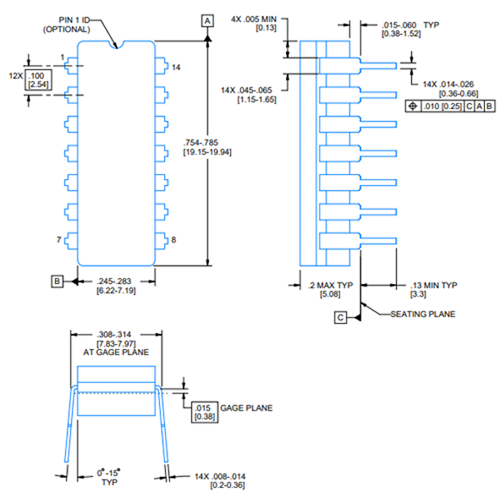
74LS73 Dual JK Flip-Flop
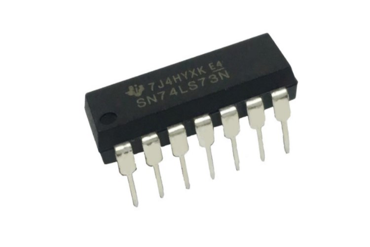
The 74LS73 is a dual in-line JK flip flop IC. It contains two independent J-K flip-flops with individual J-K, clock and direct clear inputs. The 74LS73 is a positive pulse triggered flip-flop.
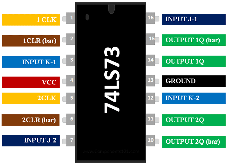
JK Flip Flop Pin Description:
|
Pin Number |
Pin Name |
Description |
|
4 |
Vcc |
Powers the IC typically with 5V |
|
13 |
Ground |
Connected to the ground of the system |
|
JK Flip Flop – 1 / JK Flip Flop - 2 |
||
|
1,5 |
Clock-1/ Clock-2 |
These pins must be provided with clock pulse for the flip flop |
|
2,6 |
Clear-1 / Clear-2 |
Resets the flip flop by clearing its memory |
|
3, 12 |
K-1/ K-2 |
Input pin of the Flip Flop |
|
16,7 |
J-1 / J-2 |
Another Input pin of the Flip Flop |
|
15, 10 |
Q-1(bar) / Q-2 (bar) |
Inverted output pin of Flip Flop |
|
14,11 |
Q-1 / Q-2 |
Output Pin of the Flip Flop |
Features of 74LS73:
- Dual JK Flip Flop Package IC
- Operating Voltage: 5V
- High Level Input Voltage: 2 V
- Low Level Input Voltage: 0.8 V
- Operating temperature range = -55 to 125°C
- Available in 14-pin PDIP, GDIP, PDSO packages
Note: Complete Technical Details can be found at the 74ls73 datasheet give at the end of this page.
Equivalent for 74LS73: MC74HC73A
Alternatives JK Flip-Flop: 74LS76, 74LS107, 4027B
Where to use 74LS73
The 74LS73 is a dual in-line JK flip flop IC. Meaning it has two JK flip flops inside it and each can be used individually based on our application. J-K input is loaded into the master while the clock is high and transferred to the slave on the high to low transition. This IC can be used in latching applications or can act as a small programmable memory for you project.
How to use 74LS73
As told earlier 74LS73 have two negative edge triggered JK flip flops, the IC is powered by +5V. The below circuit shows a typical sample connection for the working of JK flip-flop
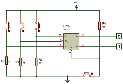
The J and K pins are the input pins for the Flip-Flop and the Q and Q bar pins are the output pins. Input pins are pulled down to ground through a 1k resistor, this way we can avoid the pin in floating condition. That is the pin will held to ground when the button is not pressed and when the button is pressed the pin will be held to supply voltage.
The reset button should be pulled up through a 1K resistor and when grounded will reset the flip-flop. The clock signal for the JK flip-flop is responsible for changing the state of the output. The flip-flop will change its output only during the rising edge of the clock signal. The clock signal here is just a push button but can be type of pulse like a PWM signal. The output state of the flip flops can be determined form the truth table below.
Normally during regular operation of the IC the reset pin will be set high and the clock pulse of known frequency will be supplied to the clock pin, then the value of J and K will be varied based on the input signals and the respective output will be obtained on the Q and Q bar pins.
Applications of 74LS73:
• Shift Registers
• Memory/Control Registers
• EEPROM circuits
• Latching devices
2D Model of 74LS73: