SN74LS164 8-Bit Shift Register
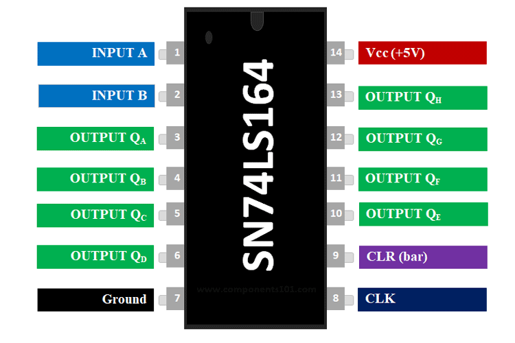
The SN74LS164 is a high-speed 8-Bit Serial-In Parallel-Out Shift Register. The input Serial data is given through a 2-Input AND gate synchronous with the LOW to HIGH transition of the clock. The IC also features gated serial inputs and an asynchronous clear pin.
Pin Description of SN74LS164
|
Pin Number |
Pin Name |
Description |
|
3, 4, 5, 6, 12, 13,14, 15 |
QA to QH |
Shift Register output Pins |
|
1, 2 |
A & B |
Parallel Input Pins |
|
6, 7 |
CLK |
Clock inputs Pin |
|
9 |
CLR |
Clear pin |
|
7 |
VSS |
Ground |
|
14 |
VCC |
Supply Voltage – 5V, 10V, 15V |
Features of SN74LS164
- An 8-bit, parallel-out serial-in Shift register
- Operating Voltage: 3V to 18V
- Supply Voltage - Max:5.25 V
- Propagation Delay Time: 25 ns
- Max. Clock Frequency: 36 MHz
- Operating Temperature Range: 0C to + 70 C
- Fully Buffered Clock
- Available in 16-pin PDIP, GDIP, PDSO packages
Note: Complete Technical Details can be found at the 74LS164 datasheet given at the end of this page.
Alternatives shift Registers
|
Name |
Type |
|
74LS379 |
Quad Parallel Shift Register |
|
4014 |
4 Bit static shift register |
|
8 Bit Shift Register |
|
|
74LS323 |
8 Bit Shift/Storage Register |
|
8-bit Shift Register |
|
|
Dual 4 Bit Static Register |
|
|
74LS299 |
8 Bit Shift/Storage Register |
Where to use SN74LS164 IC
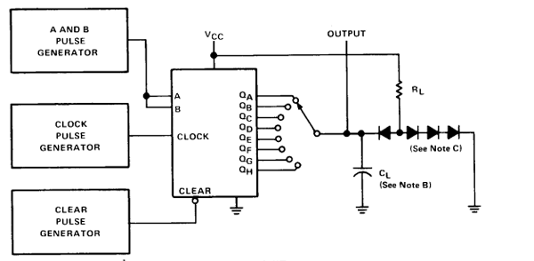
The SN74LS164 is an 8-bit serial-in, parallel-out Shift Register. Meaning it can receive (input) get data serially and control output pins in parallel. This comes in very handy where does not have enough GPIO pins on our MCU/MPU to control the required number of outputs. It is often used in projects where relatively a large number of LEDs have to be controlled through the Microcontroller. It can also be used to interface an LCD screen since it can act as the data bit for the LCD displays.
How to Use SN74LS164
The SN74LS164 shift register is commonly used with microcontrollers or microprocessors to expand the GIPO functionalities. The SN74LS164 is a 14 pin IC, it has 4 input pins, 8 output pins, power, and ground. SN74LS164 needs 4 lines of a microcontroller. One for the Clock, one for Clear, and two input pins (A & B). Input Pins A and B work as a logical AND gate, meaning if both pins are logic high (5 volts) then it will read 1. The clear pin is to clear the entire register at once.
Applications of SN74LS164
- Counters, Registers
- Arithmetic-unit registers
- Shift-left — shift right registers
- Serial-to-parallel/parallel-to-serial conversions
- Sequence generation
- Control circuits
- Code conversion
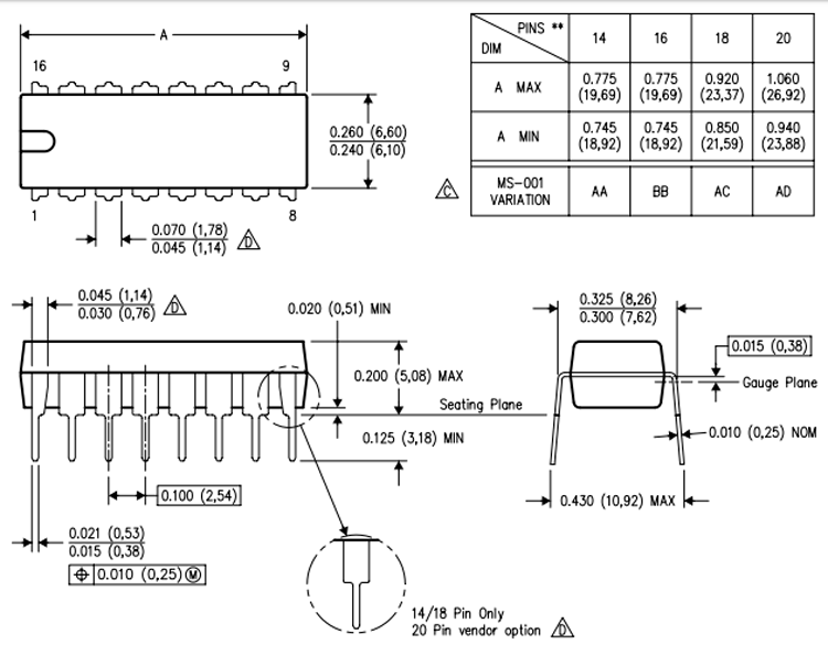
2D Model of SN74LS164 (PDIP)
Dimensions for SN74LS164 IC is given below. These dimensions are for the PDIP package. If you are using different package IC please refer to the SN74LS164 datasheet.