SN74LS13 4-Input NAND Gate Schmitt Trigger
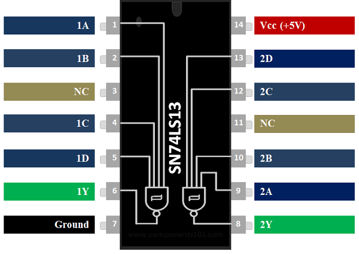
SN74LS13 Pin Configuration
|
Pin Number |
Pin Name |
Description |
|
1,2,4,5 |
1st Schmitt Input Pins |
Input pins of the NAND gate in Schmitt trigger |
|
6 |
1st Schmitt Output Pin |
Output pin of the Schmitt trigger |
|
9,10,12,13 |
2nd Schmitt Input Pins |
Input pins of the NAND gate in Schmitt trigger |
|
8 |
2nd Schmitt Output Pin |
Output pin of the Schmitt trigger |
|
7 |
Ground |
Connected to the ground of the system |
|
14 |
Vcc (+5V) |
Resets all outputs as low. Must be held high for normal operation |
Features
- 4-Input NAND gate Schmitt Trigger – Hex Inverter
- Operating Voltage: 5V
- Low Level Hysteresis voltage: 0.25V
- High Level Hysteresis voltage: 3.4V
- Output current High: -0.4mA
- Output current Low: 8.0mA
- Hysteresis voltage: 0.8V typically
- Typical Rise Time: 12nS
- Typical Fall Time: 12nS
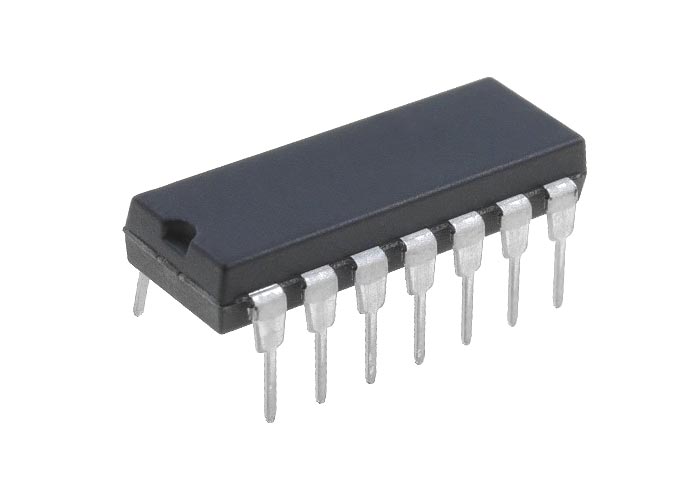
- Available in 14-pin PDIP, GDIP, PDSO packages
Note: Complete Technical Details can be found in the SN74LS13 datasheet given in the end of this page.
SN74LS13 Equivalent
74LV20A
Alternatives Schmitt Triggers
SN74LS4, CD40106, TC4584, MC14584
Where to use SN74LS13 ?
The SN74LS13 is a 4-Input NAND gate Positive Dual Schmitt trigger, meaning it has two Schmitt triggers inside it and each Schmitt trigger has 4-inputs. These 4-inputs are processed through a NAND gate and then the final output is given to the Schmitt trigger. A Schmitt trigger is used to avoid the problem of hysteresis. It can also be used to smoothen a noisy signal into sharp one. With schmitt trigger gate, we can convert sinusoidal or triangular wave to square wave. It can also be used as a logic inverter if needed. Moreover, a Schmitt trigger is also useful for debouncing multiple push buttons or other noisy input devices. The IC belongs to the legendary 74 series and has been used extensively in many circuits like FM transmitter circuit, single input LED control circuits are few to name.
Since the input is through a 4-Input NAND gate, this IC can be used for lots of creative applications, like generating various waveforms, oscillatory circuits and much more. So if you are looking for a 4-Input NAND gate Schmitt trigger, then this IC might be of interest to you.
How to Use 74LS13 ?
As mentioned earlier, 74LS13 is 4-Input NAND gate Schmitt Trigger which can be used as two individual gates. The simplified internal structure is shown in the pinouts section above.
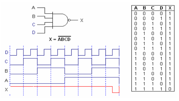
Each of these two gates can be used individually based on the application. Since the gates are fed through 4-Input NAND gate these IC have a versatile application. However because of this it might be a bit confusing to design or understand the application of this IC. The 4-Input NAND gate truth table shown below will come in handy when trying to understand how the IC works.
The unique and special functionality of a Schmitt trigger is to toggle the output based on the input signal without any noise. The input signal can be a noisy square wave or any signal wave that oscillates between the low and high hysteresis voltage.This is achieved by using a hysteresis band inside which no switching takes place. The voltage level in this band from VT+ to VT-. In our SN74LS13 IC the VT+ is 3.4V and VT- is 0.2V.
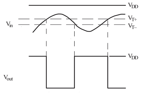
Meaning the output will get low only when the input voltage (Vin) is greater than 3.4V and will get high only when the input voltage goes below 0.2V. Any noise occurring in the input voltage between 0.2V – 3.4V will not affect the output voltage. You can use the Application report from TI to know more about using this IC
Switching Time of 74LS13
The gates in 74HC13 take some time to provide output to the given input. This time delays are called switching times. Each gate will take time to turn ON and OFF. For understanding this better let us consider the switching diagram of a gate.
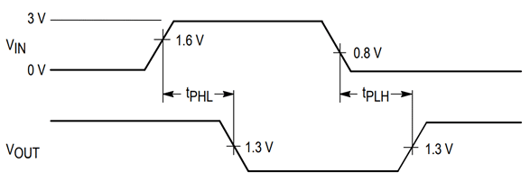
There are two delays which happen when switching. These two parameters are RISETIME (tPHL ) and FALLTIME (tPLH).
In the graph, VoH goes LOW when INPUT reaches a threshold and VoH goes HIGH when INPUT goes lower than threshold voltage. In another sense it is the output voltage.
As you can see in the graph there is time delay between LOGIC INPUT going HIGH and VoH going LOW. This delay in providing response is called RISETIME (tPHL). The RISETIME (tPHL) is 12ns.
Similarly in the graph there is time delay between LOGIC INPUT going LOW and VoH going HIGH at the OUTPUT. This delay in providing response is called FALLTIME (tPLH). The FALLTIME (tPLH) is 12ns.
Total is 24ns for each cycle. These delays must be considered at higher frequencies otherwise we will have major errors due to false triggering.
Applications
- Noise removing circuits
- Oscillatory circuits
- Waveform Generation
- Debouncing circuits
- Hysteresis controller
- Dead band filter
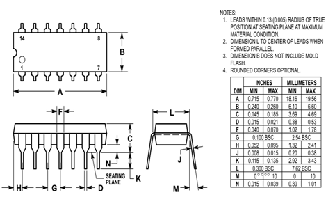
2D Model and Dimensions