NCP3064 DC-DC Converter IC
NCP3064 is a monolithic DC-DC voltage converter IC mainly used for Boost or Buck operation. This IC can be found in low voltage power supplies or any portable voltage converters. If you looking for Buck or Boost DC-DC converter upto 1.5A, this IC will be the correct choice.
|
PIN NUMBER |
PIN NAME |
DESCRIPTION |
|
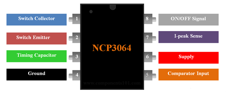
1 |
Switch Collector |
Internal Darlington switch collector |
|
2 |
Switch Emitter |
Internal Darlington switch emitter |
|
3 |
Timing Capacitor |
Timing Capacitor for Oscillator |
|
4 |
Ground |
Ground pin for all internal circuits |
|
5 |
Comparator Inverting Input |
Inverting input pin of internal comparator |
|
6 |
Vcc |
Input voltage for the IC |
|
7 |
Ipk Sense |
Peak current sensing pin |
|
8 |
ON/OFF |
ON/OFF pin. |
Features:
- Monolithic DC-DC voltage converter IC.
- Input voltage (Vin): 3V to 40V.
- Output Voltage (Vout): Adjustable
- Output Current: 1.5A (max)
- Higher operating frequency upto 150kHz.
- Logic Level Shutdown Capability.
- Cycle−by−Cycle Current Limiting.
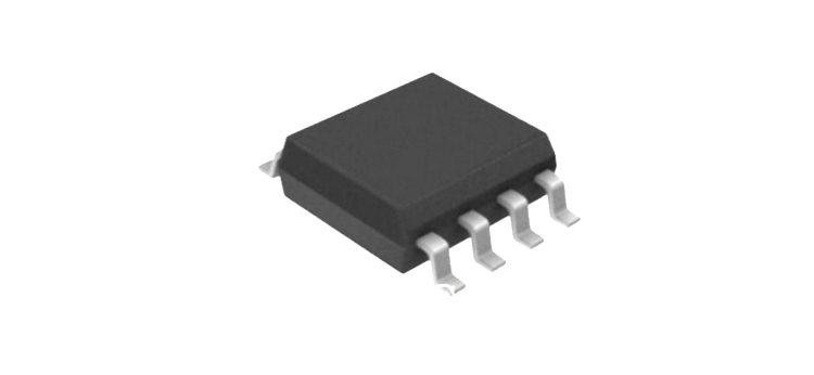
- Available in 8-pin SOIC, PDIP and DFN8 Package
Note: More technical details can be found at the datasheet linked at the bottom of this page
NCP3064 Equivalent:MC34063A, NCP3063.
Alternatives:NCP3063, TPS40200, LM2596 and XL6009.
How to use NCP3064:
As mentioned above, NCP306 is a DC-DC converter IC which can be used for buck or boost the input voltage. Each mode has separate circuits that can be found on the datasheet. The IC is available as DIP, SOIC and DFN packages from the manufacturers. This IC is the high frequency upgraded version of monolithic MC34063 series converters. In addition to the various features, this IC has logic level shutdown capability that can be used to shutdown the converter using logic signal. If the ON/OFF feature is not required, then the pin 8 of the IC can be connected to positive supply permanently. This enables the IC to be used in battery operated devices and LED driver circuits.
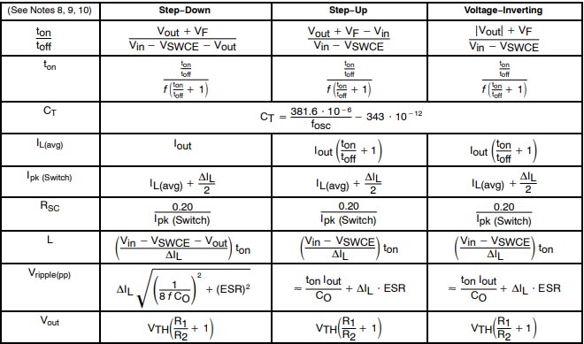
The design formula for all modes is given below.
The basic circuit for buck, boost and converter using NCP3064 is given below.
Boost circuit using NCP3064DC:
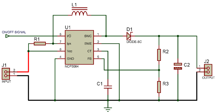
To understand the working of boost converter, we can start from the ideal basic circuit. Let us assume, initially the switch is open, then the input voltage will appear across the load. When the switch starts to conduct, the inductor is connected across the load through the switch as shown in the figure. Thus the current through the inductor starts increasing till switch is in ON state. In this state the load is disconnected from the source as the diode is reverse biased. When the switch turns OFF after certain time period, the current through the inductor interrupts thereby it generates a voltage with opposite polarity as shown in the figure. Thus the voltage generated across the inductor is added with the input voltage and it is available across the load since the diode is forward biased in this state.
Buck circuit using NCP3064:
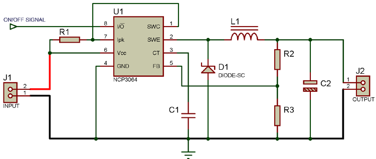
To understand the working of buck converter, let us assume initially the switch is open. Since the switch is open, the load is disconnected from the source and when the switch starts to conduct, the current flows through the inductor and to the load. The inductor starts magnetizing till the switch is ON as shown in the figure. In this state, the diode is reverse biased. When the switch turns OFF after certain time period, the current through the inductor interrupts thereby it generates a voltage with opposite polarity as shown in the figure. Thus the voltage generated across the inductor appears across the load since the diode is forward biased in this state, as the polarity of the inductor is reversed.
The voltage regulation of both converters is achieved using the feedback resistor divider. The values of the components like resistors and capacitors are calculated by using the formulae given in the table.
Applications:
- Low power DC power supplies.
- Battery operated gadgets.
- Portable electronics.
- Battery chargers.
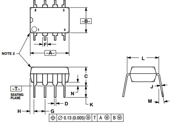
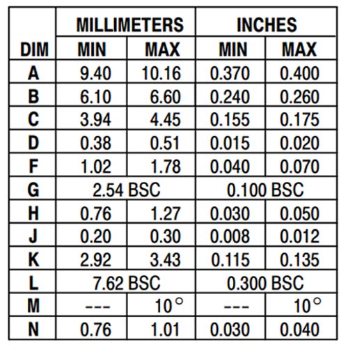
2D Model of NCP3064:
NCP3064 is available in both through hole and SMD package. The dimensions of PDIP package is shown below which can be used to create footprint for NCP3064 if you designing a PCB