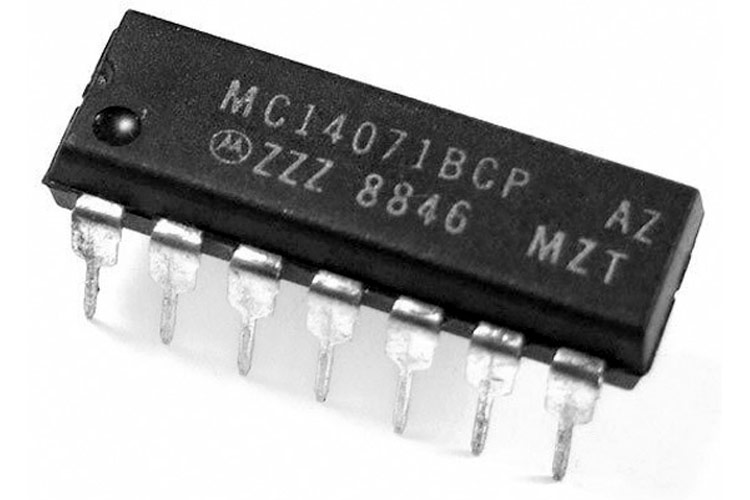
MC14071 - Quad 2-Input OR Gate IC
MC14071 IC consists of 4 independent 2-input OR gates. OR gates are used to perform logical addition operations. These are useful in building logic level circuits like Encoder, Decoders, multiplexers, etc. The IC has a wide input voltage range and is used in places where low power dissipation and high noise immunity is desired.
Features and Specifications
This section mentions some of the important features and specifications of the OR gate IC.
- Supply Voltage Range: 3V - 18V DC
- Power Dissipation: 500mW
- Input and Output current per pin: +-10mA
- Temperature Range: −55 to +125 Degree C
- Capable of Driving two Low power TTL Loads or One Low−power Schottky TTL Load
Note: More technical information can be found in the MC14071 Datasheet, linked at the bottom of this page.
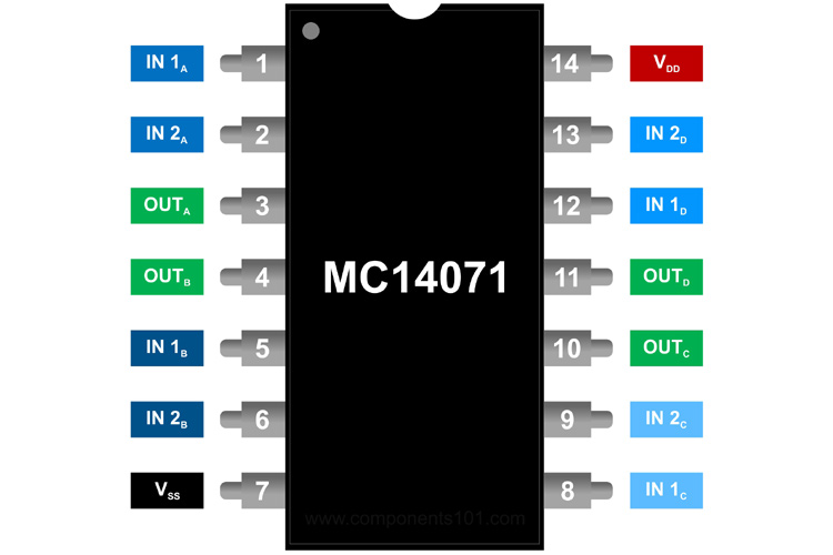
Pin Configuration
The MC14071 IC has four independent OR gates. The IC consists of 14 pins including I/O and the power pins, the table below can be referred to understand the pin configuration f the OR gate IC.
|
Pin Number |
Pin Type |
Pin Description |
|
1 |
IN1A |
Input for OR gate A |
|
2 |
IN2A |
Input for OR gate A |
|
3 |
OUTA |
Output for OR gate A |
|
4 |
OUTB |
Output for OR gate B |
|
5 |
IN1B |
Input for OR gate B |
|
6 |
IN2B |
Input for OR gate B |
|
7 |
VSS |
Ground |
|
8 |
IN1C |
Input for OR gate C |
|
9 |
IN2C |
Input for OR gate C |
|
10 |
OUTC |
Output for OR gate C |
|
11 |
OUTD |
Output for OR gate D |
|
12 |
IN1D |
Input for OR gate D |
|
13 |
IN2D |
Input for OR gate D |
|
14 |
VDD |
Positive Supply Voltage |
Working and the Boolean logic
The MC14071 IC has 4 OR logic gates inside. Each gate provides us a logical addition output of two inputs. The logic or the Boolean expression for the given logic OR gate is pretty simple. It is that for logical addition of input signals, it can also be denoted by a (+) sign. The two inputs A and B are logically added, and the result is received at the output pin. The boolean expression of the gate is: A+B=O
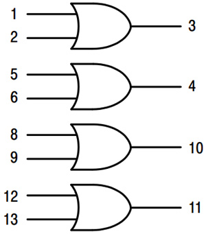
The image above explains the internal schematic of the IC. Here, in MC14071 OR gate IC Pin(1, 2, 5, 6, 8, 9, 12, 13) are presented as the input terminals whereas, Pin(3, 4, 10, 11) are the output pins where we obtain the logically added output.
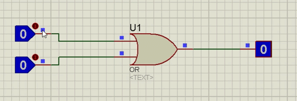
Truth table and Proteus Simulation
The truth table gives us a clearer understanding of the popper functioning of the logic gate. The logic operation of the OR gate is pretty simple. The truth table shown below shows two inputs(A and B) using the logical operation provide a corresponding output.
|
Input A |
Input B |
Output |
|
0 |
0 |
0 |
|
0 |
1 |
1 |
|
1 |
0 |
1 |
|
1 |
1 |
1 |
A simulation for the OR gate is also given-
Alternatives for MC14071 - Quad 2-Input OR Gate IC
74HC32, CD4071, CD4519, CD74HCT32M96
Available packages
SOIC−14, TSSOP−14
Applications
Here are some of the applications of the OR gate IC.
- Encoders and Decoders
- Digital Systems
- Calculators
- Basic logic circuits
2D Model
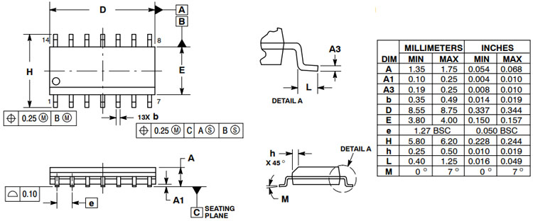
Below is the 2D model of the monostable OR gate IC along with its dimensions in millimeters and inches. The following information can be used to create custom footprints and be used while PCB designing and CAD modelling.


