MAX4173FESA Low-Cost High-Side Current Sense Amplifier
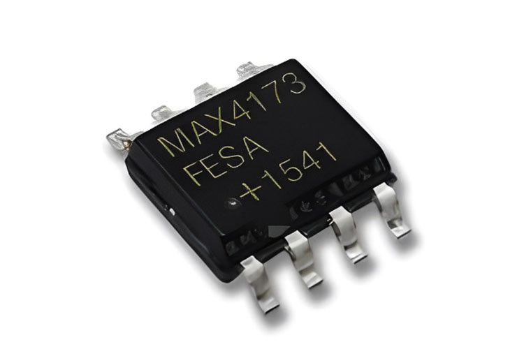
The MAX4173FESA is a low-cost, precision, high-side current sense amplifier in the SO-8 Package. It features a voltage output that eliminates the need for gain-setting resistors and is ideal for today’s notebook computers, cell phones, and other systems where current monitoring is critical. High-side current monitoring is especially useful in battery-powered systems since it does not interfere with the ground path of the battery charger. The input common-mode range of 0 to +28V is independent of the supply voltage and ensures that the current-sense feedback remains viable even when connected to a battery in deep discharge. The MAX4173FESA has a wide 1.7MHz bandwidth, making it suitable for use inside battery charger control loops. The MAX4173 operates from a single +3V to +28V supply, typically draws only 420µA of supply current over the extended operating temperature range (-40°C to +85°C)
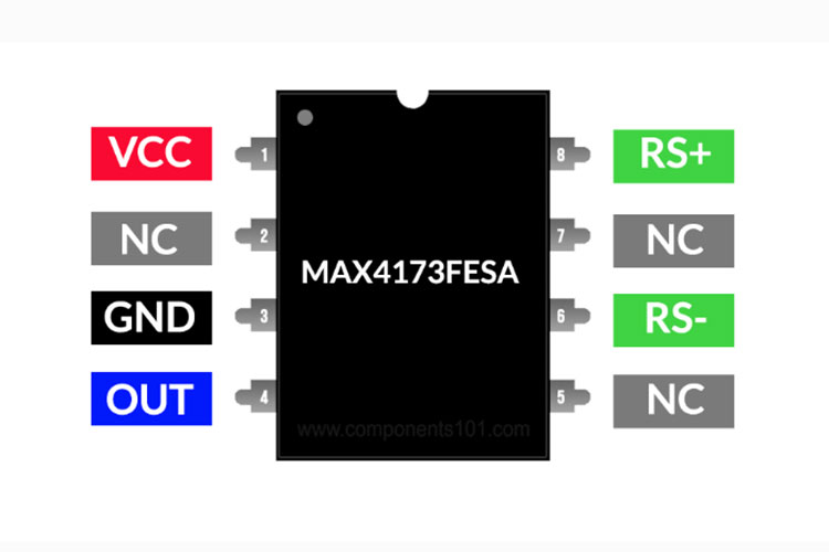
MAX4173FESA Pinout Configuration
|
Pin Number |
Pin Name |
Description |
|
1 |
VCC |
Supply Voltage Input. Bypass to GND with a 0.1µF capacitor. |
|
2 |
NC |
No Connection. Not internally connected. |
|
3 |
GND |
Ground |
|
4 |
OUT |
Voltage Output. VOUT is proportional to VSENSE ( VRS+ - VRS- ). Output impedance is approximately 12kΩ. |
|
5 |
NC |
No Connection. Not internally connected. |
|
6 |
RS- |
Load-Side Connection for the External Sense Resistor |
|
7 |
NC |
No Connection. Not internally connected. |
|
8 |
RS+ |
Power-Side Connection to the External Sense Resistor |
Features and Specifications
- Low-Cost, Compact Current-Sense Solution
- High Accuracy +2V to +28V Common-Mode Range, Functional Down to 0V, Independent of Supply Voltage
- Gain: +50V/V
- ±0.5% Full-Scale Accuracy
- ±3mV Input Offset Voltage
- Wide 1.7MHz Bandwidth
- 420µA Supply Current
Absolute Maximum Ratings
- VCC, RS+, RS- to GND: 0.3V to +30V
- OUT to GND: 0.3V to (VCC + 0.3V)
- Output Short-Circuit to VCC or GND: Continuous
- Differential Input Voltage (VRS+ - VRS-): ±0.3V
- Current into Any Pin: ±20mA
- Continuous Power Dissipation (TA = +70°C)
- 8-Pin SO (derate 5.88mW/°C above +70°C): 471mW
- Operating Temperature Range: -40°C to +85°C
- Storage Temperature Range: -65°C to +150°C
- Lead Temperature (soldering, 10s): +300°C
- Soldering Temperature (reflow): +260°C
Note: Complete technical details can be found in the MAX4173FESA datasheet at this page’s end.
How To Use MAX4173FESA?
The schematics below show the typical application diagram of a MAX4173FESA.
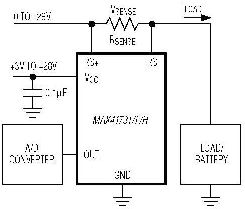
To measure lower currents more accurately, use a high value for RSENSE. The high value develops a higher sense voltage that reduces offset voltage errors of the internal op amp. In applications monitoring very high currents, RSENSE must be able to dissipate the I2R losses. If the resistor’s rated power dissipation is exceeded, its value may drift or it may fail altogether, causing a differential voltage across the terminals more than the absolute maximum ratings. If ISENSE has a large high-frequency component, minimize the inductance of RSENSE. Wire-wound resistors have the highest inductance, metal-film resistors are somewhat better, and low-inductance metal-film resistors are best suited for these applications. The table below shows the recommended values for the current sense resistor.
|
FULL-SCALE LOAD CURRENT ILOAD (A) |
CURRENT-SENSE RESISTOR RSENSE (mΩ) |
GAIN |
FULL-SCALE OUTPUT VOLTAGE (FULL-SCALE VSENSE = 100mV) VOUT (V) |
|
0.1 |
1000 |
20 |
2.0 |
|
50 |
5.0 |
||
|
100 |
10.0 |
||
|
1 |
100 |
20 |
2.0 |
|
50 |
5.0 |
||
|
100 |
10.0 |
||
|
5 |
20 |
20 |
2.0 |
|
50 |
5.0 |
||
|
100 |
10.0 |
||
|
10 |
10 |
20 |
2.0 |
|
50 |
5.0 |
||
|
100 |
10.0 |
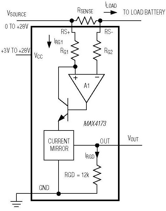
Functional Block Diagram
Applications
- Cell Phones
- General System/Board-Level Current Monitoring
- Notebook Computers
- PA Bias Control
- Portable Battery-Powered Systems
- Power-Management Systems
- Precision Current Sources
- Smart Battery Packs/Chargers
DC Characteristics
|
PARAMETER |
SYMBOL |
CONDITIONS |
MIN |
TYP |
MAX |
UNITS |
|
|
Operating Voltage Range |
V |
|
|
|
28 |
V |
|
|
Common-Mode Input Range |
VCMR |
|
0 |
|
28 |
V |
|
|
Common-Mode Rejection |
CMR |
VRS+ > +2.0V |
|
90 |
|
dB |
|
|
Supply Current |
|
|
|
0.42 |
1 |
mA |
|
|
Leakage Current |
0.3 |
3 |
µA |
||||
|
Input Bias Current |
IRS+ |
VRS+ > +2.0V |
0 |
|
50 |
µA |
|
|
VRS+ ≤ +2.0V |
-350 |
|
50 |
||||
|
IRS- |
VRS+ > +2.0V |
0 |
|
100 |
|||
|
VRS+ ≤ +2.0V |
-700 |
|
100 |
||||
|
Full-Scale Sense Voltage |
VSENSE |
VSENSE = VRS+ - VRS- |
|
150 |
|
mV |
|
|
Total OUT Voltage Error |
|
VSENSE = +100mV, VCC = +12V, VRS+ = +12V |
|
±0.5 |
5.75 |
% |
|
|
VSENSE = +100mV, VCC = +12V, VRS+ = +12V,TA = +25°C |
|
0.5 |
3.25 |
||||
|
VSENSE = +100mV, VCC = +28V, VRS+ = +28V |
|
0.5 |
5.75 |
||||
|
VSENSE = +100mV, VCC = +12V, VRS+ = +0.1V |
|
-9 |
±24 |
||||
|
VCC = +12V, VRS+ = +12V, VSENSE = +6.25mV |
|
±7.5 |
|
||||
|
Out High Voltage |
|
MAX4173F, VCC = +7.5V, VRS+ = 28V,VSENSE = 250mV |
|
0.8 |
1.2 |
V |
|
|
OUT Low Voltage |
VOL |
VCC = +5V, VRS+ = 0.89V,VSENSE = 0mV |
TA = +25°C |
|
1.2 |
5 |
mV |
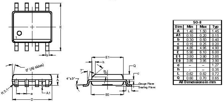
2D Model and Dimensions