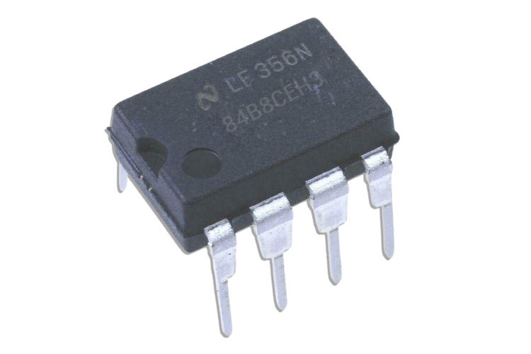
LF356 JFET Input Op-Amp IC
LF356 is an op-amp that has a JFET input. These JFET Op-amps are an excellent choice for low noise applications using High or Low source impedance. Having a JFET at the input side increases the bandwidth gain and reduces the input noise of the IC. The IC has a wide bandwidth, fast settling time, and very low voltage and current noise, making it ideal for pre-amplification devices.
Features and Configurations
This section discusses some of the important features and specifications of the LF356 JFET Input Op-Amp IC.
- Gain Bandwidth: 5 MHz
- Operational Voltage: +-15V
- Offset Voltage: 2 mV max
- Input Bias Current: 30pA
- Amplifier Type: JFET
- Low Supply Current: 3.6mA
- Low Total Harmonic Distortion: <0.02%
Note: More technical information can be found in the LF356 IC Datasheet, linked at the bottom of this page.
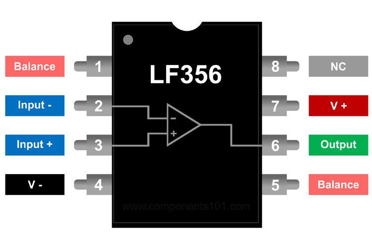
Pin Configuration
The LF356 JFET Input Op-Amp IC has 8 I/O pins. The table below shows the Pin Number, its type, and its description.
|
Pin Number |
Pin Type |
Pin Description |
|
1 |
Balance |
Balance for input offset voltage |
|
2 |
-Input |
Inverting input |
|
3 |
+Input |
Non-Inverting input |
|
4 |
V- |
Negative power supply |
|
5 |
Balance |
Balance for input offset voltage |
|
6 |
Output |
Output pin |
|
7 |
V+ |
Positive power supply |
|
8 |
NC |
No Connection |
Typical application circuit/Working and internal schematic of LF356 Op-Amp IC
An output of an Operational Amplifier is the product of the gain and the input voltage.
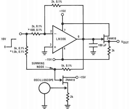
The circuit shows a typical application for the LF356 Op-Amp. This op-amp can be used at several places and has a plethora of applications. Whenever the voltage at the non-inverting input(+) is greater than the voltage at the inverting input(-) the output we get is a HIGH, whereas if the voltage at inverting is greater than the non-inverting terminal the output we get is a LOW.
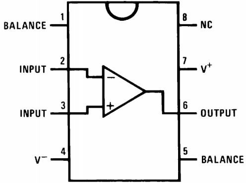
The diagram above explains the internal schematic of the LF356 IC. As we have already discussed, the IC having 8 pins. The Op-amp is connected only through pin 2 and 3 as the input and provides an output at pin 6. Pin 2 is the inverting input and Pin 3 is the non-inverting input. Pin 1 and 5 are the balance pins to set the input offset voltage.
Alternatives for LF356 JFET Input Op-Amp IC
Available packages
SOIC(8-PIN), TO-CAN(8-PIN), PDIP(8-PIN)
Applications
Here are some of the applications of LF356 JFET Input Op-Amp IC.
- Fast A/D and D/A converters
- Logarithmic Amplifiers
- Photocell Amplifiers
- Sample and Hold Circuits
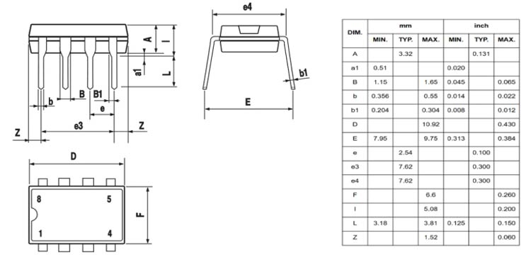
2D Model
Below is the 2D model of the LF356 JFET Input Op-Amp IC along with its dimensions in millimeters and inches. You can use the following information to design custom footprints of the IC and use it to for PCB designing and CAD modelling.