INA226 Ultra-Precise I2C Output Current, Voltage and Power Monitor
The INA226 is a current and power monitor chip with high-accuracy ADC and a resolution of 16bit. It features I2C and SMBUS-compatible interfaces for easy integration and monitors both shunt voltage drop and bus voltage drop. Programmable calibration value, conversion times, and averaging, combined with an internal multiplier enables direct readout of current in amperes and power in watts. The INA226 senses current on common-mode bus voltages that can vary from 0 V to 36 V, independent of the supply voltage. The device operates from a single 2.7 V to 5.5 V supply, drawing a typical 330 µA of supply current. The device is specified over the operating temperature range between -40°C and +125°C and features up to 16 programmable addresses on the I2C-compatible interface.
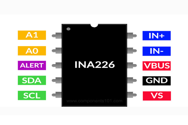
INA226 Pinout Configuration
|
PIN NAME |
PIN NO. |
I/O |
DESCRIPTION |
|
A0 |
2 |
Digital input |
Address pin. Connect to GND, SCL, SDA, or VS. Table 2 shows pin settings and corresponding addresses. |
|
A1 |
1 |
Digital input |
Address pin. Connect to GND, SCL, SDA, or VS. Table 2 shows pin settings and corresponding addresses. |
|
Alert |
3 |
Digital output |
Multi-functional alert, open-drain output. |
|
GND |
7 |
Analog |
Ground. |
|
IN+ |
10 |
Analog input |
Connect to the supply side of the shunt resistor. |
|
IN– |
9 |
Analog input |
Connect to the load side of the shunt resistor. |
|
SCL |
5 |
Digital input |
Serial bus clock line, open-drain input. |
|
SDA |
4 |
Digital I/O |
Serial bus data line, open-drain input/output. |
|
VBUS |
8 |
Analog input |
Bus voltage input. |
|
VS |
6 |
Analog |
Power supply, 2.7 V to 5.5 V. |
Features
- Senses bus voltages from 0 V to 36 V
- High-side or low-side sensing
- High accuracy
- 0.1% gain error (max)
- 10 µV offset (max)
- Reports current, voltage, and power
- Configurable averaging options
- 16 programmable addresses
- Operates from 2.7 V to 5.5 V power supply
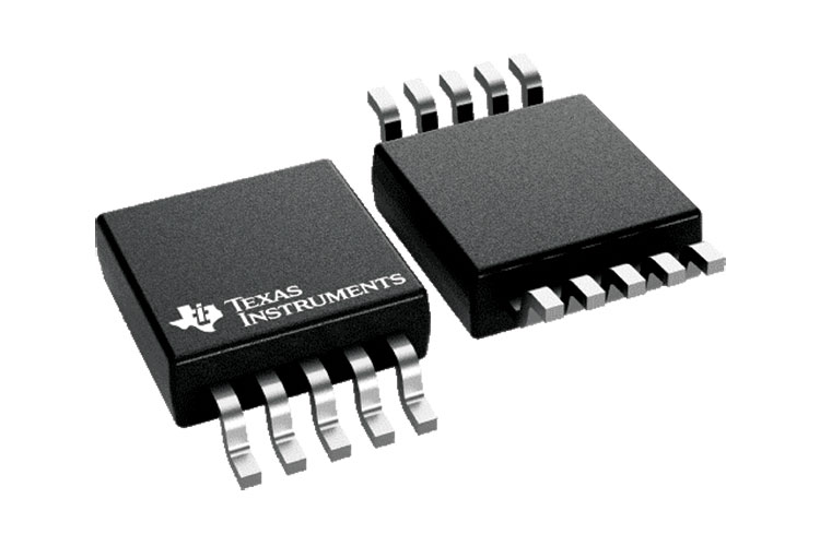
- 10-pin, DGS (VSSOP) package
Note: Complete technical details can be found in the INA226’s datasheet at this page’s end.
How To Use INA226?
The schematics below shows the typical application circuit diagram of INA226.
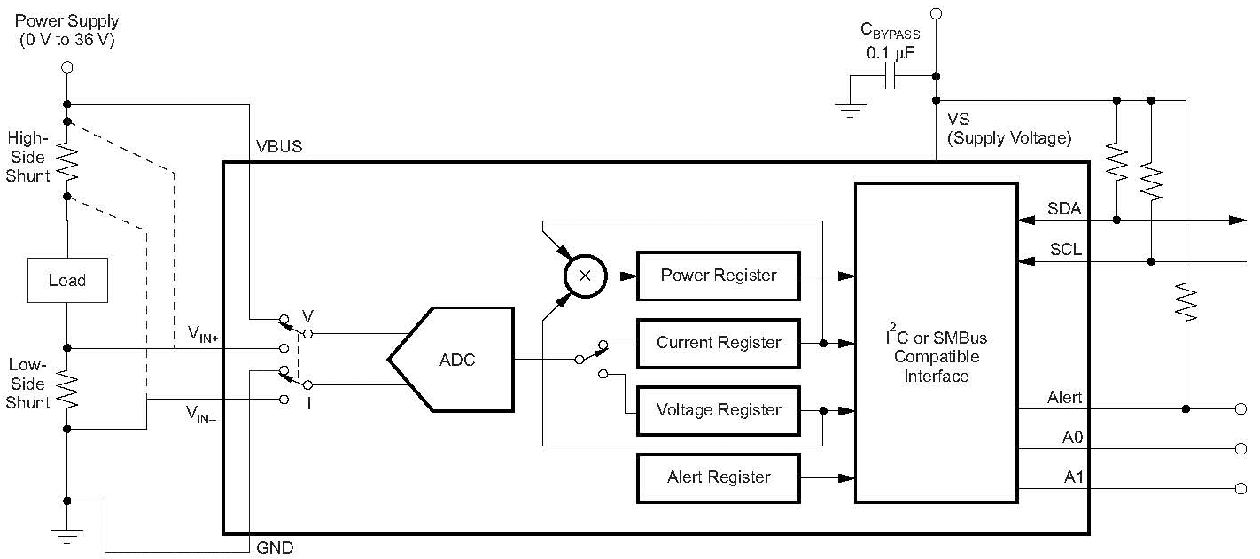
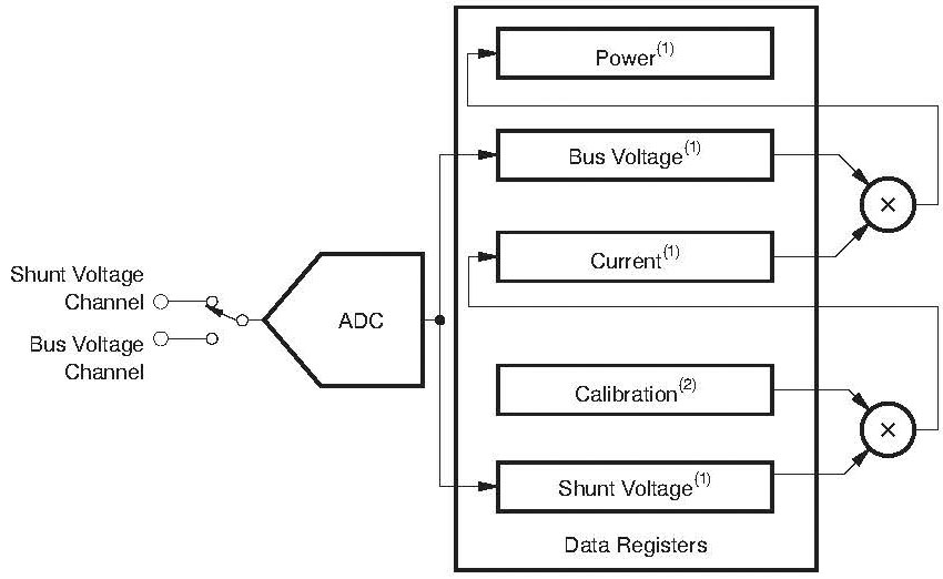
The INA226 device performs two measurements on the power-supply bus of interest. The voltage developed from the load current that flows through a shunt resistor creates a shunt voltage that is measured at the IN+ and IN– pins. The device can also measure the power supply bus voltage by connecting this voltage to the VBUS pin. The differential shunt voltage is measured with respect to the IN–pin while the bus voltage is measured with respect to the ground. The device is typically powered by a separate supply that can range from 2.7 V to 5.5 V. The bus that is being monitored can range in voltage from 0 V to 36 V, based on the fixed 1.25-mV LSB for the Bus Voltage Register that a full-scale register results in a 40.96 V value.
Functional Block Diagram
Applications
- Servers
- Telecom equipment
- Computing
- Power management
- Battery chargers
- Power supplies
- Test equipment
Absolute Maximum Ratings
|
|
|
MIN |
MAX |
UNIT |
|
VVS |
Supply voltage |
|
6 |
V |
|
Analog Inputs, IN+, IN– |
Differential (VIN+ – VIN-)(2) |
–40 |
40 |
V |
|
Common-Mode (VIN+ + VIN-) / 2 |
–0.3 |
40 |
||
|
VVBUS |
|
–0.3 |
40 |
V |
|
VSDA |
|
GND – 0.3 |
6 |
V |
|
VSCL |
|
GND – 0.3 |
VVS + 0.3 |
V |
|
IIN |
Input current into any pin |
|
5 |
mA |
|
IOUT |
Open-drain digital output current |
|
10 |
mA |
|
TJ |
Junction temperature |
|
150 |
°C |
|
Tstg |
Storage temperature range |
–65 |
150 |
°C |
DC Characteristics
|
PARAMETER |
TEST CONDITIONS |
MIN |
TYP |
MAX |
UNIT |
|
|
INPUT |
||||||
|
|
Shunt voltage input range |
|
–81.9175 |
|
81.92 |
mV |
|
|
Bus voltage input range(1) |
|
0 |
|
36 |
V |
|
CMRR |
Common-mode rejection |
0 V ≤ VIN+ ≤ 36 V |
126 |
140 |
|
dB |
|
VOS |
Shunt offset voltage, RTI(2) |
|
|
±2.5 |
±10 |
μV |
|
|
Shunt offset voltage, RTI(2) vs temperature |
–40°C ≤ TA ≤ 125°C |
|
0.02 |
0.1 |
μV/°C |
|
PSRR |
Shunt offset voltage, RTI(2) vs Power supply |
2.7 V ≤ VS ≤ 5.5 V |
|
2.5 |
|
μV/V |
|
VOS |
Bus offset voltage, RTI(2) |
|
|
±1.25 |
±7.5 |
mV |
|
|
Bus offset voltage, RTI(2) vs temperature |
–40°C ≤ TA ≤ 125°C |
|
10 |
40 |
μV/°C |
|
PSRR |
Bus offset voltage, RTI(2) vs power supply |
|
|
0.5 |
|
mV/V |
|
IB |
Input bias current (IIN+, IIN– pins) |
|
|
10 |
|
μA |
|
|
VBUS input impedance |
|
|
830 |
|
kΩ |
|
|
Input leakage (3) |
(IN+ pin) + (IN– pin),Power-down mode |
|
0.1 |
0.5 |
μA |
|
DC ACCURACY |
||||||
|
|
ADC native resolution |
|
|
16 |
|
Bits |
|
|
1 LSB step size |
Shunt voltage |
|
2.5 |
|
μV |
|
Bus voltage |
|
1.25 |
|
mV |
||
|
|
Shunt voltage gain error |
|
|
0.02% |
0.10% |
|
|
|
Shunt voltage gain error vs temperature |
–40°C ≤ TA ≤ 125°C |
|
10 |
50 |
ppm/°C |
|
|
Bus voltage gain error |
|
|
0.02% |
0.10% |
|
|
|
Bus voltage gain error vs temperature |
–40°C ≤ TA ≤ 125°C |
|
10 |
50 |
ppm/°C |
|
|
Differential nonlinearity |
|
|
±0.1 |
|
LSB |
|
SMBus |
||||||
|
|
SMBus timeout(4) |
|
|
28 |
35 |
ms |
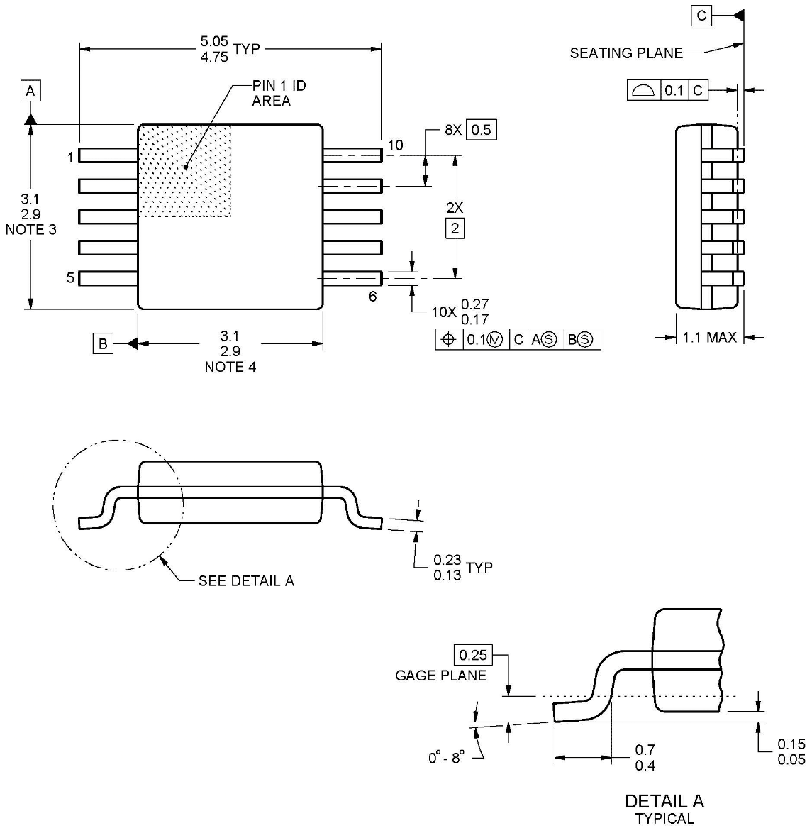
2D Model and Dimensions