CD4066 Quad Bilateral Switches – Multiplexer
The CD4066 is a Quad Bilateral Switch IC, that is, it has four switches which can be controlled individual using a control pin. These switches can conduct in both the directions making it bilateral, it is commonly used for multiplexing analog or digital signals. The switches have very low internal resistance making it suitable for audio applications.
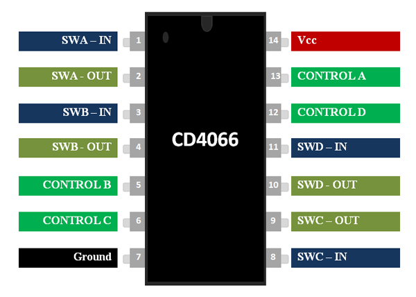
Pin Configuration
|
Pin Number |
Pin Name |
Description |
|
1, 3, 8, 11 |
Switch Input A,B,C,D |
Input pins for the four bilateral switches |
|
2, 4, 9, 10 |
Switch Output A,B,C,D |
Output pins for the four bilateral switches |
|
5, 6, 12, 13 |
Control A,B,C,D |
Control pins for the four bilateral switches |
|
7 |
Ground |
Ground pin of the IC |
|
14 |
Vcc |
Pin to power the IC |
Features
- Quad Bilateral Switch for Multiplexing
- Very Low Internal Resistance
- Operating Voltage: 3V to 18V
- Switching Voltage: 20V (maximum)
- On-state Resistance: 5Ω (at 15V Vcc and 10kΩ Load)
- Output current High: -0.4mA
- Low Level Control pin Voltage: 0.9V (max)
- High Level Control pin Voltage: 11V (min @ 15V Vcc)
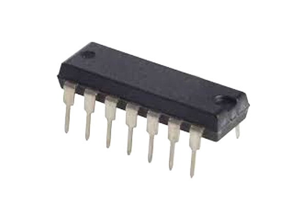
- Available in 14-pin PDIP, GDIP, PDSO packages
Note: Complete Technical Details can be found at the CD4066 datasheet given at the end of this page.
CD4016 Equivalents
CD4016, CD4068
Alternatives multiplexer
Where to use CD4066B IC
The CD4066 is a bi-directional analog switching IC similar to CD4016, it is commonly used in multiplexing applications; it can also be used to isolate signals. The switch is bilateral and hence can be used for both digital and analog signals. The IC can operate from 3V to 18V, but commonly operated at 5V, 10Vor 15V nominal voltages. It can switch voltages upto 20V (peak).
Difference between CD4066 and CD4016
Both the CD4066 and CD4016 are very similar IC that shares the same pinouts. Hence one can act as a direct pin to pin replacement for the other. However the major difference between both is that CD4066 has very low internal resistance, according to the datasheet it can only 5Ω of on-state resistance as compared with 200Ω of CD4016 IC. Hence the CD4066 is used in places where weak signals are involved like audio signals or in places where higher switching efficiency is needed.
How to Use CD4066 IC
The CD4066 has four bilateral switches that can be controlled independently using a digital signal. Each switch has two Input/output pins called SWx-IN and SWx-OUT. Both of which can be used as a input or output pin, they can also be used to switch variable voltages like PWM wave, sine wave etc of low magnitude and frequency. These two pins will can be controlled by the CONTROLx pin. The below simulation shows one out of the four switches in the IC.
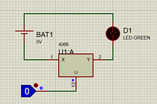
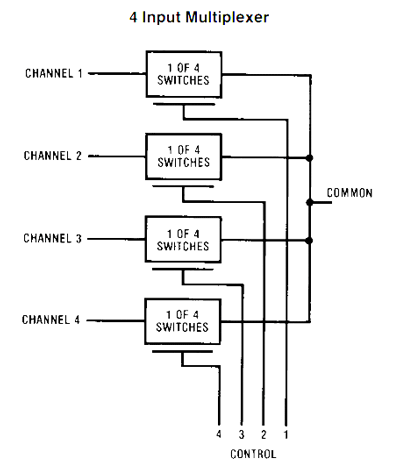
As you can see here the two switch pins are named X and Y and the control pin is named as C. By default when control pin is logic 0 (0V) the switch is open (not connected), but when a control signal is given to control pin C the switch closes and the LED glows. You can also use this IC as a 4-Input multiplexer by combining all the four switches to a common point as shown below.
Applications
- 4-Input Multiplexer
- Sample and Hold circuits
- Network switching
- Dead band filter
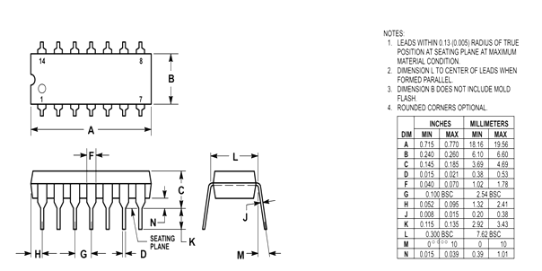
2D Model