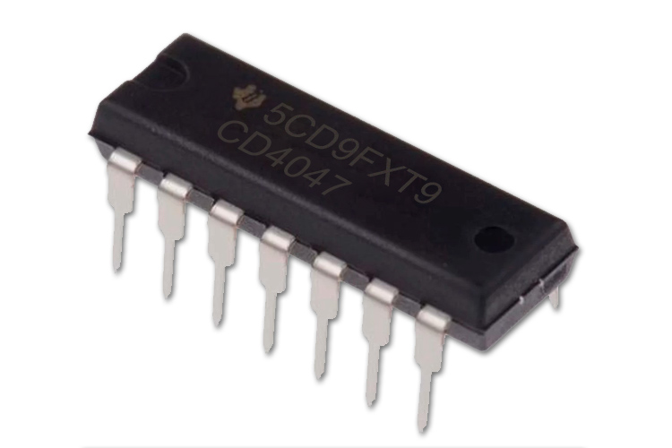
CD4047 Monostable/Astable Multivibrator IC
The CD4047 is a low-powered monostable/astable multivibrator IC. The CD4047 IC allows a positive or negative edge-triggered monostable multivibrator mode with retriggering and external counting options.
Key Features
- Low power consumption: special CMOS oscillator for low power configuration.
- Operating modes: unstable (one-shot) Mode and Astable (free-running) Mode.
- Only one external R and C required.
- Supply voltage range: 3.0V to 15V.
- Maximum Power Dissipation(Pd): 700mW in DIP Package and 500mW in SOIC package.
- Operating Temperature Range: -40°C to +85°C
Note: More technical information can be found in the CD4047 Datasheet, linked at the bottom of this page.
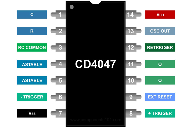
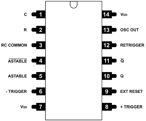
CD4047 Pinout Configuration
The CD4047 consists of 14 pins for both- a small outline integrated circuit and a dual-inline package. The following table shows the pin description of each pin.
|
Pin Number |
Pin Name |
Pin Description |
|
1 |
C |
Can be connected to an external capacitor |
|
2 |
R |
Can be connected to an external resistor |
|
3 |
R-C COMMON |
Common pin to connect with resistor and capacitor |
|
4 |
ASTABLE BAR |
Set to Low when used in astable mode |
|
5 |
ASTABLE |
Set to high when used in astable mode |
|
6 |
-TRIGGER |
High to Low transition needs to be applied when used in monostable mode |
|
7 |
VSS |
Ground Pin |
|
8 |
+TRIGGER |
Low to High transition needs to be applied when used in monostable mode. |
|
9 |
EXT RESET |
An external reset signal can be provided to this pin. |
|
10 |
Q |
Generates high output. |
|
11 |
Q BAR |
Provides an inverse output of pin 10 |
|
12 |
RETRIGGER |
Used to simultaneously retriggering the pins 6 and 8 |
|
13 |
OSC OUT |
Generated Oscillated output |
|
14 |
VDD |
Voltage Supply Pin |
Alternatives
CD4047BCMX, CD4047BCM, CD4047BCN
How to use the CD4047 IC in Monostable Mode
The CD4047 IC can be operated in monostable and astable modes. It can be operated as a monostable mode by connecting a capacitor between the pins 1 and 3.
Monostable Mode: A LOW-HIGH transition at pin 8 (+TRIGGER) and a HIGH-LOW transition at pin 6 (-TRIGGER) is needed to obtain the monostable operation. This IC can be retriggered by applying a LOW-HIGH transition to both the pins 8 and 12 (RETRIGGER).
Circuit Diagram of CD4047 IC in Monostable Mode
The basic circuit diagram for Monostable mode configuration is shown below. You can also check out our CD4047 Working, Formula, and Simulation article to get a deeper understanding of different working modes of CD4047 and how to use them practically .
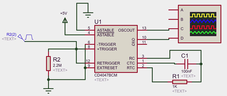
In the above circuit the pin 8 (+TRIGGER) is connected to a pulse generator which will provide a LOW-HIGH transition and a HIGH-LOW transition at pin 6 (-TRIGGER) can be provided by connecting this pin to the ground through the External Reset pin 9 (EXTRESET). The pin 4 (ASTABLE BAR) is set to HIGH by providing an external 5V power supply. A capacitor (100nF) is connected in between pin 1 and pin 3.
How to use the CD4047 IC in Astable Mode
In astable mode, an external resistor needs to be connected between pins 2 and 3 to determine the output frequency.
Astable Mode: Astable operation can be started by applying a HIGH level on pin 5 (ASTABLE) and a LOW level on pin 4 (ASTABLE Bar). The output frequency is determined at pin 10 (Q) and 11 (Q bar) by the timing components.
Circuit Diagram of CD4047 IC in Astable Mode
The basic circuit diagram for Astable mode configuration is shown below.
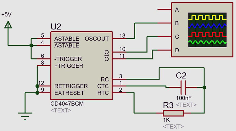
In the above circuit, the pin 5 (ASTABLE), pin 4 (ASTABLE BAR), and pin 6 (-TRIGGER) is connected to an external 5V power supply which will provide a LOW-HIGH transition and a HIGH-LOW transition at pin 6 (-TRIGGER) can be provided by connecting this pin to the ground through the External Reset pin 9 (EXTRESET). The pin 4 (ASTABLE BAR) is set to HIGH by providing an external 5V power supply. An external resistor (resistance is 1K ohm) is connected in between pin 2 and pin 3.
Applications
The primary applications of the CD4047 IC are given below.
- Envelope Detection
- Frequency Multiplication
- Frequency Division
- Time Delay Circuits
- Frequency Discriminators
- Timing Circuits
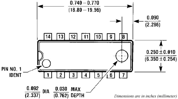
2D Model and Dimensions
The 2D model in this section consists of the module's dimensions in millimeters. This information can be used for designing custom footprints of the module, which can be used for PCB designing and CAD modelling.