CD4014 Static 8-Stage Shift Register

The CD4014BC is an 8-stage parallel input/serial output shift register. A parallel/serial control input enables individual JAM inputs to each of 8 stages. Q outputs are available from the sixth, seventh and eighth stages. CD4014 have common CLOCK and PARALLEL/SERIAL CONTROL inputs, a single SERIAL data input, and individual parallel "JAM" inputs to each register stage.
Pin Description of CD4014:
|
Pin Number |
Pin Name |
Description |
|
1, 4, 5, 6, 7, 13, 14, 15 |
PI-1 to PI-8 |
Parallel Inputs |
|
2, 3, 12 |
Q6, Q7, Q8 |
Outputs |
|
10 |
CLOCK |
Clock Input |
|
9 |
P/S |
Parallel/Serail Control |
|
11 |
Serial IN |
Serial input Pin |
|
8 |
VSS |
Groung |
|
16 |
Vdd (Vcc) |
Supply Voltage – 5V, 10V, 15V |
Features of CD4014:
- 8-stage parallel input/serial output shift register
- Operating Voltage: 3V to 18V
- Propagation Delay Time: 320 ns
- Maximum input current of 1 µA at 18 V
- Number of Input Lines: 9
- Number of Output Lines: 3
- Operating Temperature Range:- 55 C to + 125 C
- Available in 16-pin PDIP, GDIP, PDSO packages
Note: Complete Technical Details can be found at the CD4014 datasheet give at the end of this page.
Alternatives shift Registers:
|
Name |
Type |
|
74LS379 |
Quad Parallel Shift Register |
|
Parallel In/Parallel out Shift Register |
|
|
74LS166 |
8 Bit Shift Register |
|
74LS323 |
8 Bit Shift/Storage Register |
|
74LS164 |
S/P Shift Register |
|
Dual 4 Bit Static Register |
|
|
74LS299 |
8 Bit Shift/Storage Register |
Where to use CD4014 IC
The CD4014 is an 8-stage parallel input/serial output shift register. Meaning it can receive (input) data in parallel and control 4 output pins in parallel. This comes in very handy where you do not have enough GPIO pins on our MCU/MPU to control the required number of outputs. It is often used in projects where relatively a large number of LED’s has to be controlled through the Microcontroller. It can also be used to interface LCD screen since they can acts as the data bit for the LCD displays.
How to Use CD4014:
The CD4014 is an 8-stage CMOS Static Shift Register having common clock and parallel/serial control inputs, single serial data input and individual parallel JAM inputs to each register stage. Connection diagram for CD4014 IC is given below.
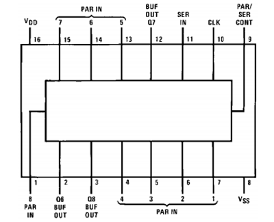
In CD4014 each register stage is D-type, master-slave flip-flop. The pins 4, 5, 6, 7 and 8, 13, 14, 15 are parallel input pins and pins 2, 3 and 12 output pins. In which pin 1 is the clock which sends a constant pulse to keep timing. When the parallel/serial control input is in the logical “0” state, data is serially shifted into the register synchronously with the positive transition of the clock. When the parallel/ serial control input is in the logical “1” state, data is jammed into each stage of the register synchronously with the positive transition of the clock.
Applications of CD4014:
- Parallel input/serial output data queueing
- Parallel to serial data conversion
- General-purpose register
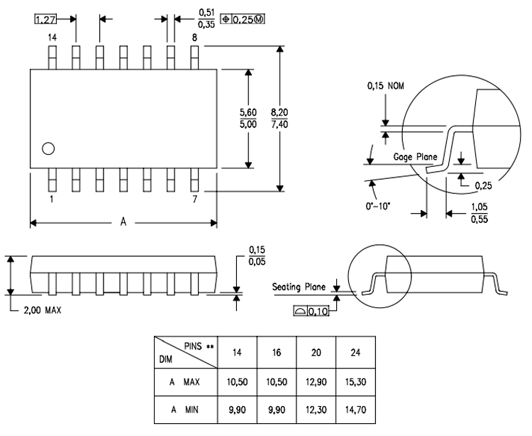
2D Model of CD4014 (PDSO):