CD4012 Dual 4-Input NAND Gate
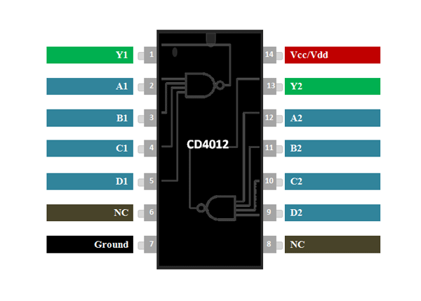
The CD4012 is a CMOS technology based, 4-input NAND gate Dual package, i.e. the IC has two NAND gates which can operate independently and each gate can take in four Inputs. It is commonly used in buffer circuits, logic inverter circuits etc.
Pin Description
|
Pin Number |
Pin Name |
Description |
|
1 |
NAND Gate Output pin (1) |
Output pin of NAND Gate - 1 |
|
2,3,4,5 |
NAND Gate Input pin (1) |
Four Input pins of NAND Gate -1 |
|
7 |
Ground |
Connect to the ground of the circuit. |
|
9,10,11,12 |
NAND Gate Input pin (2) |
Four Input pins of NAND Gate -2 |
|
13 |
NAND Gate Output pin (2) |
Output pin of NAND Gate - 2 |
|
14 |
Vcc (Vdd) |
Used to power the IC. Typically +5V is used |
Features
- Four Input OR Gate – Dual Package
- Typical Operating Voltage: 5V
- Operating Voltage Range: 3V to 15V
- Power Dissipation: 500mW
- Minimum logic Low voltage @+5V: 0.05V
- Minimum Logic High voltage @+5V: 4.95V
- Propagation Delay @5V : 50ns (maximum)
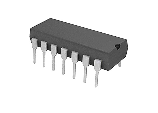
- Available in 14-pin PDIP, GDIP, PDSO packages
Note: Complete Technical Details can be found at the CD4012 datasheet given at the end of this page.
CD4012 Equivalents
74HC20, 74S140
Other Logic Gates
74LS00, 74LS08, 74LS02, 74LS04, 74HCT04
Where to use CD4012 IC
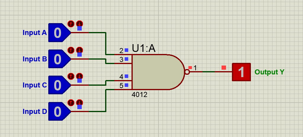
The CD4012 is 4-Input NAND Gate IC. It can take in four logic inputs and provide an output based on the truth table. Since the NAND gate is a universal gate it can also be combined to act as other gates like NOT gate, AND gate etc. NAND gate is commonly used in buffer circuits and logic inverter circuits for digital communication.
4-Input NAND Gate Truth Table
As told earlier the Output acts based on the truth table which is given below. Let us consider the four inputs A,B,C and D and the output as J. The output J will follow the logic expression Y=
|
Input A |
Input B |
Input C |
Input D |
Output Y |
|
|
0 |
0 |
0 |
0 |
1 |
|
|
0 |
0 |
0 |
1 |
1 |
|
|
0 |
0 |
1 |
0 |
1 |
|
|
0 |
0 |
1 |
1 |
1 |
|
|
0 |
1 |
0 |
0 |
1 |
|
|
0 |
1 |
0 |
1 |
1 |
|
|
0 |
1 |
1 |
0 |
1 |
|
|
0 |
1 |
1 |
1 |
1 |
|
|
1 |
0 |
0 |
0 |
1 |
|
|
1 |
0 |
0 |
1 |
1 |
|
|
1 |
0 |
1 |
0 |
1 |
|
|
1 |
0 |
1 |
1 |
1 |
|
|
1 |
1 |
0 |
0 |
1 |
|
|
1 |
1 |
0 |
1 |
1 |
|
|
1 |
1 |
1 |
0 |
1 |
|
|
1 |
1 |
1 |
1 |
0 |
|
How to use CD4012 IC
To use the CD4012 IC, just power it using the Vcc (pin 14) and ground (pin 8) lines. The typical operating voltage of the IC is +5V, but it can also be operated in +5V, +10V and +15V. The output voltage of the IC on the pin Y will be equal to the operating voltage of the IC. As per the truth table shown above, when either one or both the input of the Gate is high the output will be high. The complete working of the gate with a sample circuit is shown in the GIF file below.
Applications
- Logic Buffer circuit
- Basic Logic Circuits
- Encoders and Decoders
- Multiplexers and De-multiplexers
- Oscillator circuits
- Networking and Digital Systems
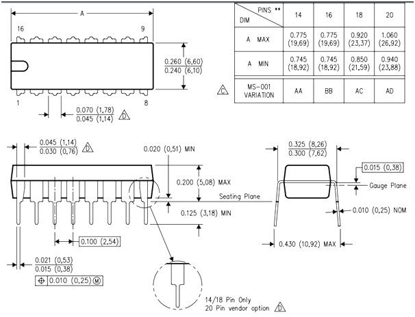
2D-Model