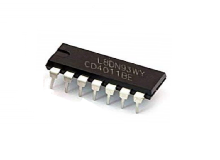
CD4011 CMOS 2-Input NAND Gate
CD4011 is a member of the CD40xx CMOS IC series. The CD4011 IC contains four independent NAND gates. The devices perform the Boolean function Y = A × B or Y = A + B in positive logic. This IC is used in AV Receivers, Portable Audio Docks, and Blu-Ray Players.
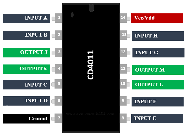
Pin Description of CD4011:
|
Pin Number |
Pin Name |
Description |
|
1,2,5,6,8,9,12,13 |
NAND Gate Input pins |
First Input pin for the NAND gate |
|
3,4,10,11 |
NAND Gate Output pins |
Output pin for the NAND gate |
|
7 |
Ground |
Connect to the ground of the circuit. |
|
14 |
Vcc (Vdd) |
Used to power the IC. Typically +5V is used |
Features of CD4011:
- Dual Input NAND Gate – Quad Package
- Typical Operating Voltage: 5V
- High-Level Output Current:- 1.5 mA
- Low-Level Output Current: 1.5mA
- Propagation Delay Time:60 ns
- Operating Temperature Range:- 55 C to + 125 C
- Available in 14-pin PDIP, GDIP, PDSO packages
Note: Complete Technical Details can be found at the CD4011 datasheet give at the end of this page.
CD4011 NAND Gate Equivalents: SN74HC00, SN54LS00
Where to use the CD4011 IC?
CD4011 is a 2-input 4 NAND gate IC and used in many electronic circuits. CD4011 used for performing the Logic NAND function. When you want to use it as a logic inverter, NAND gates in this chip can be reconfigured to make them NOT gate. So we can make SN54LS00 a four NOT gate chip if necessary. It can be used where high-speed NAND operation is necessary. This chip has less transition times which are needed for high-speed applications. So SN54LS00 can be used in high-frequency systems.
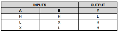
2-input NAND Gate Truth Table
How to Use CD4011 IC
As mentioned earlier CD4011 has four NAND gates. The internal circuit of CD4011 with four NAND gates is shown below.
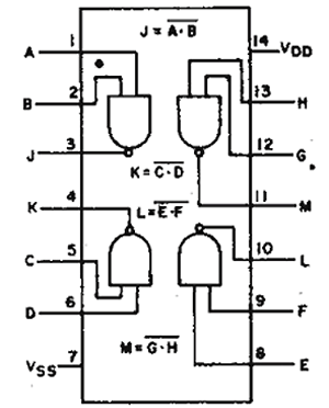
CD4011 has 12 input-output pins for four NAND gates. To use the CD4011 IC, just power it using the Vcc and ground pins. The typical operating voltage of the IC is +5V, but it can also be operated in +7V. The output voltage of the IC on the output pin will be equal to the operating voltage of the IC. As per the NAND gate truth table, when both the input of the Gate is Low the output will be high, otherwise, it will be low.
Applications of CD4011
- AV Receivers
- Portable Audio Docks
- Blu-Ray Players
- Home Theater
- MP3 Players or Recorders
- Personal Digital Assistants (PDAs)
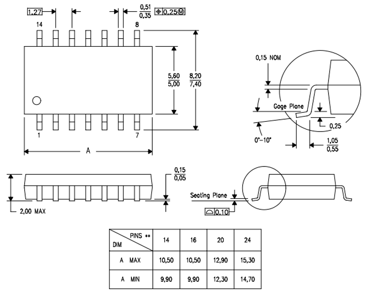
2-D Model of CD4011 (PDSO)
Dimensions for CD4011 is given below. These dimensions are for the PDSO package. If you are using different package IC please refer to the CD4011 datasheet.