AT24C32 Two-Wire Serial EEPROM
24C32 is a 4K x 8 (32Kbit) Serial Electrically Erasable PROM. This IC is specially designed for advanced, low power applications such as personal communications or data acquisition. It is available in the standard 8-pin plastic DIP, and 8-pin surface mount SOIC packages.
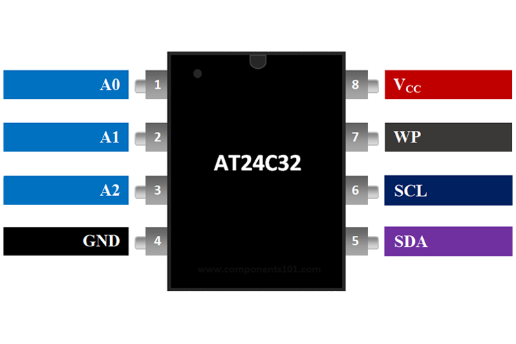
AT24C32 Pinout Configuration
|
Pin Number |
Pin Name |
Description |
|
1,2,3 |
A0,A1,A2 |
User configured Chip Select pins, useful during cascading |
|
4 |
Vss (Ground) |
Connected to the ground of the circuit |
|
5 |
Serial Data (SDA) |
Serial Data pin for I2C Communication |
|
6 |
Serial Clock (SCL) |
Serial Clock pin for I2C Communication |
|
7 |
WP (Write Protect) |
If connected to Vss write is enabled, if connected to Vcc write is disabled. |
|
8 |
Vcc |
Connect to supply rail |
AT24C32 Specifications & Features
- Supply Voltage: 1.8V to 5.5V
- Supply Current - Max: 2 mA
- Memory Size: 32 Kbit
- Organization: 4 k x 8
- Interface Type: Serial, 2-Wire, I2C
- Maximum Clock Frequency: 40 kHz
- 32-Byte Page Write Mode
- Self-timed write cycle
- Available in 8-pin PDIP, SOIC and TSSOP packages
Note: Complete Technical Details can be found at the 24C32 datasheet given at the end of this page.
Equivalent for AT24C32: 24LC512, 24C04
Alternatives EEPROM’S: 24LC1026, 25LC050, AT24C256
Where to Use AT24C32
The AT24C32 EEPROM IC provides 32 bits of serial electrically erasable and programmable read-only memory (EEPROM). The device’s cascadable feature allows up to 8 devices to share a common 2-wire bus. This IC has an operating voltage range from 1.8V to 5.5V, which makes it ideal to be used for both 3.3V and 5V systems. The AT24C32 comes with a memory space of 32Kbit and works 2-Wire Serial Interface.
So if you are looking to use an EEPROM IC where low-power and low-voltage operation are essential, then this IC might be the right choice for you.
How to Use AT24C32 IC
Interfacing AT24C32 with a microcontroller is very easy as you only require to connect 5 pins. The interfacing diagram for AT24C32 IC is shown below.
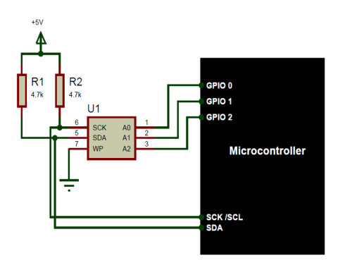
The Serial Clock SCK (pin 6) is connected to the Serial clock pin of the microcontroller, and the Serial Data SDA (pin 5) is connected to the Serial Data pin of the microcontroller. Also like all I2C communication, SCK and SDA pins are pulled high using two pull-up resistors or while 4.7k. This will keep the bus at high state during the idle condition.
Chip select pins (A0, A1, and A2) are useful only if more than one I2C device or EEPROM is connected to the same microcontroller, else three pins can be grounded directly. In the above diagram, we have connected the three pins to the GPIO pins so that we can cascade more than one EEPROM IC if required.
The Write Protect WP (pin 7) is provided for improving data security in the IC. The data can be written or erased on the EEPROM only if the WP pin is held low (logic 0). Else the data written on the EEPROM will remain as such. Normally this pin will be grounded (logic 0) when the protection is not needed. Data can be read from the EEPROM at all conditions irrespective of the status of the WP pin.
Applications of AT24C32 IC
- Data Logging
- Audio devices
- Remote storage devices
- Data analytics
- Storage devices
- Used where Flash memory of MCU is less
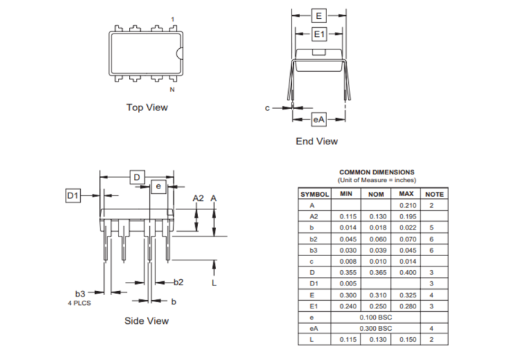
2D-Model of AT24C32 IC
Dimensions for AT24C32 IC is given below. These dimensions are for the 8-Pin PDIP package. If you are using a different package IC, please refer to the AT24C32 datasheet.