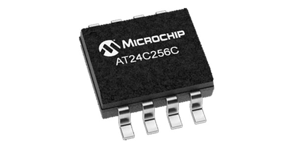
AT24C256C 256-Kbit I2C EEPROM
The AT24C256 is a 32K byte, 8-pin EEPROM IC. As we know EEPROM stands for Electrically Erasable Programmable Read-Only Memory, we can store information on this IC and it will remain there even when the power is turned off just like your pen drive. Then the information can be retrieved or over-written when required.
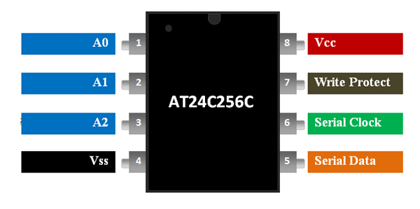
Pin Configuration
|
Pin Number |
Pin Name |
Description |
|
1,2,3 |
A0,A1,A2 |
User configured Chip Select pins, useful during cascading |
|
4 |
Vss (Ground) |
Connected to the ground of the circuit |
|
5 |
Serial Data (SDA) |
Serial Data pin for I2C Communication |
|
6 |
Serial Clock (SCL) |
Serial Clock pin for I2C Communication |
|
7 |
Write-Protect |
If connected to Vss write is enabled, if connected to Vcc write is disabled. |
|
8 |
Vcc |
Connect to supply rail |
AT24C256 Specifications
- 256Kbit EEPROM IC
- Operating Voltage: 1.7V to 5.5V
- 2-wire Serial Interface (IIC)
- 32K byte of storage memory (256Kbit)
- 128-byte page write buffer
- Read current: 40uA
- Write cycle time: 5ms
- 400kHz to 1MHz clock compatible
- 10,00,000 read/write cycles
- Available in 8-pin VFBGA, UDFN and TSSOP packages.
AT24C256 Equivalent
Alternatives EEPROM
24C04, 24LC1026, 25LC040, 24C32
AT24C256 EEPROM Overview
AT24C256 EEPROM has a wide operating voltage range from 1.7V to 5.5V, which makes it ideal to be used both for 3.3V systems and 5V systems. Each IC comes with a storage space of 32Kbyte and can be cascaded with 8 similar IC if expansion is required. The IC works with help of 2-wire protocol (IIC/I2C) and hence it is easy to interface with most of the MCUs and consumes less number of pins. Also the Read current for the IC is only 40uA which makes it ideal for battery operated applications.
This IC is not available in the DIP package and is only available as SMD component, so if you are beginner you might want to look at 24LC512 which comes in DIP package.
How to use AT24C256 EEPROM IC
The AT24C256 EEPROM IC communicates with help of I2C protocol. To interface it with a MCU just power the IC (usually with 3.3V or 5V) and connect the communication lines as shown below.
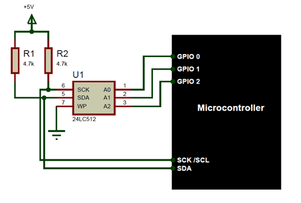
The Serial Clock SCK (pin 6) is connected to the Serial clock pin of the microcontroller and the Serial Data SDA (pin 5) is connected to the Serial Data pin of the microcontroller. Also like all I2C communication we have pulled the SCK and SDA line high using two pull-up resistors or while 4.7k. This will keep the bus at high state during idle condition.
Other than that we have three chip select pins namely A0, A1 and A2. These three pins are useful only if more than one I2C device or EEPROM is connected to the same microcontroller, else three pins can be grounded directly. In the above diagram we have connected the three pins to the GPIO pins so that we can cascade more than one EEPROM IC if required.
The Write Protect WP (pin 7) is provided for improving data security in the IC. The data can be written or erased on the EEPROM only if the WP pin is held low (logic 0). Else the data written on the EEPROM will remain as such. Normally this pin will be grounded (logic 0) when the protection is note needed. Data can be read from the EEPROM at all conditions irrespective of the status of the WP pin.
Once the communication is successful the MCU can be programmed to read/write data to the EEPROM by calling the right register values. First the address of the location to which the data must be read/written should be specified followed by the data. Normally this is how data will be read/written byte by byte. The 24LC512 IC provides an option called page write which allows the user to write 128-bytes of data continuously without mention the address of each data.
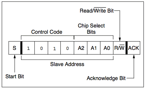
The above figure tells how the data is exchanged between the microcontroller and the EEPROM IC. The total message can be split into Start bit, Slave address, Read/Write Bit and then acknowledge bit. Further the Slave address is split into Control code and chip select bits. The control code is hardcoded and cannot be changed by us hence the value will always be 1010. The value of Chip Select bits is set by the MCU. For example if all the three pins A2,A1 and A0 are made low the resulting address of the device will be 0x50. Read the data sheet at the end of the page to know more on how to communicate with the IC.
Applications
- Data Logging
- Audio devices
- Remote storage devices
- Data analytics
- Storage devices
- Used where Flash memory of MCU is less
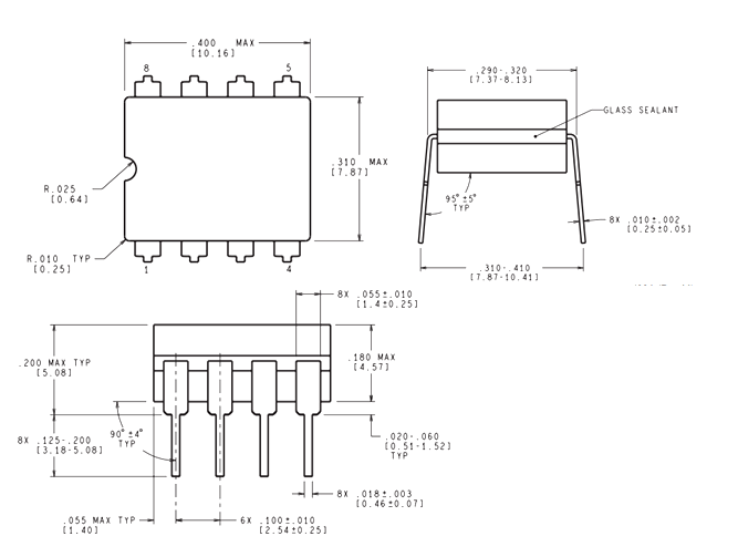
2D-Model