AD7791 Low Power 24-Bit Sigma-Delta ADC

The AD7791 is a low-power, low-noise, 24-bit sigma-delta analog-to-digital converter (ADC) from Analog Devices. It's commonly used in precision measurement applications due to its high resolution and low noise characteristics. The AD7791 comes with an internal clock so we can avoid the external clock signal. The output data rate can be programmed, and we can set that from 9.5Hz to 120Hz. The device can operate from a 3V power supply while operating in 3V the power consumption is only about 225uW. The AD7791 uses a serial interface for communication with a microcontroller or other digital system. The IC is available in a 10-pin MSOP Package.
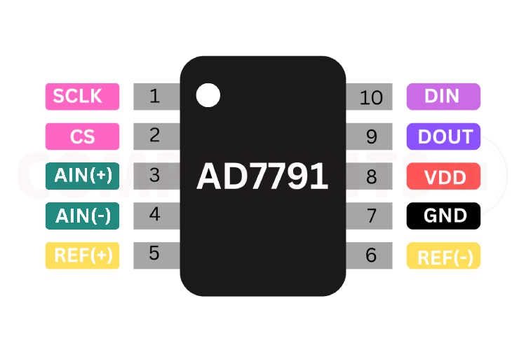
AD7791 Pinout Configuration
Here are the pinout details for AD7791.
| PIN NO | PIN NAME | DESCRIPTION |
| 1 | SCLK | Serial Clock Input |
| 2 | CS | Chip Select Input |
| 3 | AIN(+) | Analog Input. |
| 4 | AIN(–) | Analog Input |
| 5 | REFIN(+) | Positive Reference Input |
| 6 | REFIN(–) | Negative Reference Input |
| 7 | GND | Ground |
| 8 | VDD | Supply Voltage |
| 9 | DOUT/RDY | Serial Data Output/Data Ready Output. |
| 10 | DIN | Serial Data Input |
Features of AD7791
AD7791 ADC has the following key features:
- INPUT -2.5 V to 5.25 V
- LOW CURRENT CONSUMPTION: 75 μA max Power-down: 1 μA max
- RMS noise: 1.1 μV at 9.5 Hz update rate 19.5-bit p-p resolution (22 bits effective resolution)
- Integral nonlinearity: 3.5 ppm typical Simultaneous 50 Hz and 60 Hz rejection
- Internal clock oscillator
- Rail-to-rail input buffer
- VDD monitor channel.
- Temperature range: –40°C to +105°C
- 10-lead MSOP
How to Identify AD7791?
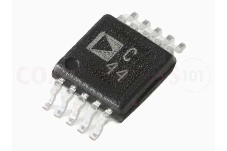
The AD7791 comes with 2 different markings, COT and C44.
Manufacturers of AD7791:
The AD7791 is manufactured by Analog Devices. There are no alternative manufacturers for the same part number as of the date of writing this article.
AD7791 Equivalents
If you are looking for an equivalent or replacement for AD7791 you may check out AD7790 and AD7792 from the same family.
AD7791 Alternatives
If you are looking for an alternative for AD7791 you can look at the other IC from these.
HX711, MCP3008, ADS1115, ADC0804, MCP3301, ADC0831, ADS1015, LTC2400
Note: Complete technical details can be found in the AD7791 datasheet at this page’s end.
AD7791 Schematics
The following image shows the AD7791 application circuit diagram.
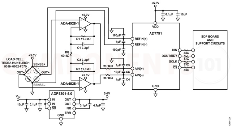
The circuit above is a precision weigh scale signal conditioning system. It uses the AD7791, a low-power buffered 24-bit sigma-delta ADC along with two external ADA4528-1 zero-drift amplifiers. This solution allows for high DC gain with a single supply. Ultralow noise, low offset voltage, and low drift amplifiers are used at the front end for amplification of the low-level signal from the load cell. The circuit yields a 15.3-bit noise-free code resolution for a load cell with a full-scale output of 10 mV. This circuit allows great flexibility in designing a custom low-level signal conditioning front end that gives the user the ability to easily optimize the overall transfer function of the combined sensor-amplifier-converter circuit. The AD7791 maintains good performance over the complete output data range, from 9.5 Hz to 120 Hz, which allows it to be used in weigh scale applications that operate at various low speeds.
Troubleshooting Tips for AD7791
- The circuit’s performance is not stable: There is a lot of noise introduced to the line.: Ensure that the power supply to the AD7791 is stable and within the specified voltage range. Each VCC terminal should have a good bypass capacitor to prevent power disturbance. Should use 0.1-μF bypass capacitor in reference lines.
- Not getting any signals from the IC: Make sure that the AD7791 is powered correctly according to the specified voltage levels and current requirements. Double-check all the connections, including SPI lines, reference voltage inputs, and analog input signals, to ensure they are properly connected. Verify that the clock signal to the AD7791 is within the specified frequency range and has the correct waveform.
- SPI communication is not working: First check the hardware connections. Check whether the spi pins are connected correctly to the microcontroller. Then check the programming side like bit order and clock phase.
Design tips for AD7791
How to minimize noise while using AD7791?
Good decoupling is important when using high-resolution ADCs. VDD should be decoupled with 10 µF tantalum in parallel with 0.1 µF capacitors to GND. To achieve the best from these decoupling components, they should be placed as close as possible to the device, ideally right up against the device. All logic chips should be decoupled with 0.1 µF ceramic capacitors to DGND.
Is the ADP7791 sensitive to ESD?
Yes. The performance and working of the IC are well affected by ESD.
How to order ADP7791?
You can check with your supplier with the following part numbers, AD7791BRM, AD7791BRMZ, AD7791BRM-REEL and AD7791BRMZ- REEL. These are all 10 MSOP packages, the only difference is how they are supplied and their markings.
What are the design considerations when designing a PCB using AD7791?
The printed circuit board that houses the AD7791 should be designed so that the analog and digital sections are separated and confined to certain board areas. A minimum etch technique is generally best for ground planes because it gives the best shielding. It is recommended that the AD7791’s GND pin be tied to the AGND plane of the system. In any layout, the user must keep in mind the flow of currents in the system, ensuring that the return paths for all currents are as close as possible to the paths the currents took to reach their destinations. Avoid forcing digital currents to flow through the AGND sections of the layout. The AD7791’s ground plane should be allowed to run under the AD7791 to prevent noise coupling. The power supply lines to the AD7791 should use as wide a trace as possible to provide low impedance paths and reduce the effects of glitches on the power supply line. Fast-switching signals such as clocks should be shielded with digital ground to avoid radiating noise to other sections of the board, and clock signals should never be run near the analog inputs. Avoid crossover of digital and analog signals. Traces on opposite sides of the board should run at right angles to each other. This will reduce the effects of feedthrough through the board. A microstrip technique is by far the best, but it is not always possible with a double-sided board. In this technique, the component side of the board is dedicated to ground planes, while signals are placed on the solder side.
Applications of AD7791
- Smart transmitters
- Battery applications
- Portable instrumentation
- Sensor measurement
- Temperature measurement
- Pressure measurement.
- Weigh scales.
- 4 to 20 mA loops
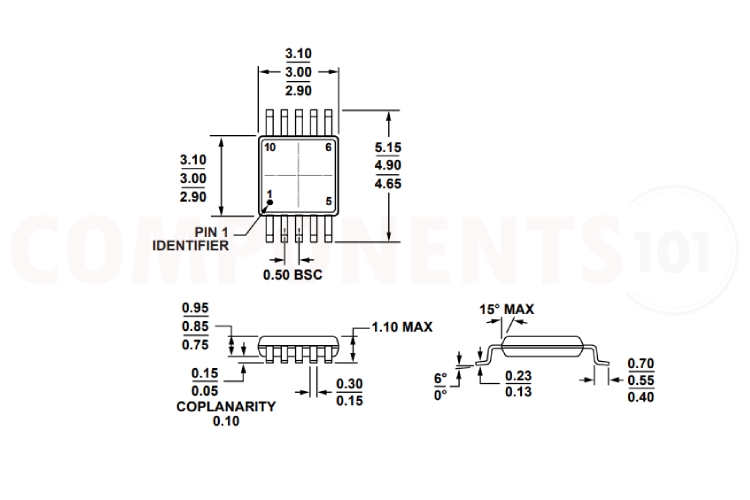
2D Model and Dimensions of AD7791
Here you can find the mechanical drawings of AD7791 along with its dimensions. The dimensions can be used to create custom footprints of the module and be used for PCB or CAD modelling.