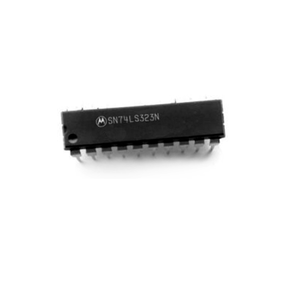
74LS323 8-bit Shift/Storage Register
The 74LS323 is an 8-Bit Universal Shift/Storage Register with 3-state outputs. Its function is similar to the 74LS299 with the exception of Synchronous Reset. Parallel load inputs and flip-flop outputs are multiplexed to minimize pin count.
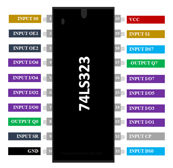
74LS323 Pinout Configuration
|
Pin Number |
Pin Name |
Description |
|
1, 19 |
S0 & S1 |
Mode Select Input Pins |
|
3, 4 |
OE1 & OE2 |
3-State Output Enable (active LOW) Inputs |
|
4, 5, 6, 7, 13, 14 ,15 ,16 |
I/O0 to I/O7 |
Parallel Data Input or Parallel Output (3-State) |
|
8, 17 |
Q0 & Q7 |
Serial Outputs |
|
9 |
SR |
Synchronous Reset (active LOW) Input |
|
11 |
DS0 |
Serial Data Input for Right Shift |
|
18 |
DS7 |
Serial Data Input for Left Shift |
|
12 |
CP |
Clock Pulse Input |
|
7 |
VSS |
Ground |
|
14 |
VCC |
Supply Voltage – 5V, 10V, 15V |
Features of 74LS323 IC
- Supply Voltage - Max: 5.25 V
- Operating Supply Voltage: 4.75 V to 5.25 V
- Output Type: 3-State
- Operating Temperature Range: 0 C to + 70 C
- Max. Clock Frequency: 25 MHz
- Maximum Propagation Delay Time: 39ns @5V
- Common I/O for Reduced Pin Count
Note: Complete Technical Details can be found at the 74LS323 datasheet given at the end of this page.
Alternatives shift Registers:
|
Name |
Type |
|
74LS379 |
Quad Parallel Shift Register |
|
4014 |
4 Bit static shift register |
|
8 Bit Shift Register |
|
|
8-bit Shift Register |
|
|
Dual 4 Bit Static Register |
|
|
74LS299 |
8 Bit Shift/Storage Register |
Where to use 74LS323 IC
The 74LS323 is an 8-bit universal Shift/Storage Register. This comes in common I/O pins for reduced pin count. It is often used in projects where relatively a large number of LEDs have to be controlled through the Microcontroller. It can also be used to interface LCD screens since they can act as the data bit for the LCD displays.
How to Use 74LS323
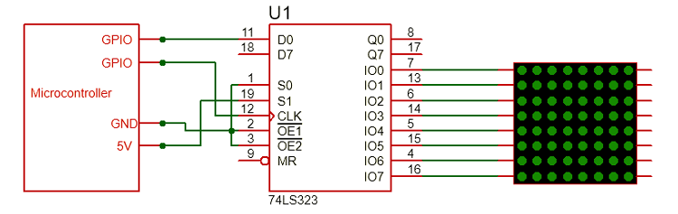
The 74LS323 shift register is commonly used with microcontrollers or microprocessors to expand the GIPO functionalities. Two function-select inputs (S0, S1) and two output-control inputs (Q0, Q7) can be used to choose the modes of operation. Synchronous parallel loading is accomplished by taking both function-select lines, S0 and S1, high. A simple application circuit diagram is shown below. In the circuit, I/O pins are connected to a led dot matrix display and D0 and clock pins are connected to GPIO pins of a microcontroller.
Applications of 74LS323:
- Counters, Registers
- Arithmetic-unit registers
- Shift-left-shift-right registers
- Serial-to-parallel/parallel-to-serial conversions
- Sequence generation
- Control circuits
- Code conversion


