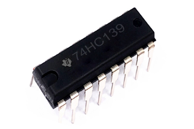
74HC139 2 to 4 Decoder/Demultiplexer IC
Features and Specifications
This section mentions some of the important features and specifications of the 74HC139 IC.
- Operating Voltage Range: 2 V - 6 V DC
- Outputs Can Drive up to Ten LSTTL Loads
- Low input current: 1uA
- Incorporate Two Enable Inputs to Simplify Cascading and/or Data Reception
- ±4-mA Output Drive at 5 V
- Active LOW mutually exclusive outputs
Note: More technical information can be found in the 74HC139 Datasheet, linked at the bottom of this page.
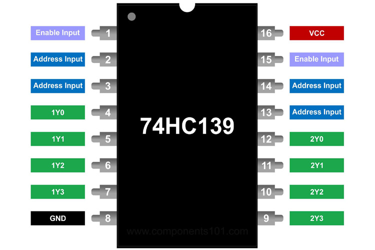
74HC139 Pinout Configuration
The decoder/demultiplexer IC consists of 16 pins, the table below can be referred to understand the pin configuration of the IC.
|
Pin Number |
Pin Type |
Pin Description |
|
1 |
1G |
Enable Input(Active Low) |
|
2 |
1A |
Address Input |
|
3 |
1B |
Address Input |
|
4 |
1Y0 |
Output(Active Low) |
|
5 |
1Y1 |
Output(Active Low) |
|
6 |
1Y2 |
Output(Active Low) |
|
7 |
1Y3 |
Output(Active Low) |
|
8 |
GND |
Ground |
|
9 |
2Y3 |
Output(Active Low) |
|
10 |
2Y2 |
Output(Active Low) |
|
11 |
2Y1 |
Output(Active Low) |
|
12 |
2Y0 |
Output(Active Low) |
|
13 |
2B |
Address Input |
|
14 |
2A |
Address Input |
|
15 |
2G |
Enable Input(Active Low) |
|
16 |
VCC |
Positive supply voltage |
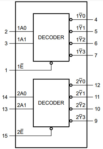
Working Principle and Functional Diagram of the Decoder/Demux IC
The IC consists of 2 mutually exclusive decoders with address inputs (nA0, nA1), outputs (nY0 to nY3), and enable pins as shown in the logical diagram below.
The IC can work either as a decoder or a demux. If the Enable pin(E’) is connected to the ground it works as a decoder whereas, if the Enable pin is connected to the VCC pin it will work as a Demultiplexer. The 2 to 4 Decoder means that it has 2 input lines and 4 output lines along with an enable pin. The output pins for this decoder IC are active low, which means we will have an inverted output. So for the normal operation of the decoder IC, the E’ pin should be zero or grounded.
The truth table shown below explains how the IC works under certain given input parameters.
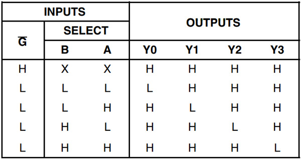
[G’/E’ = Enable pin, A,B/1A0,1A1,2A0,2A1 = Select lines(Input), Y0,Y1,Y2,Y3 = Output pins]
The connections to the decoder/demux IC are pretty simple. Based upon the needs, the enable pin can be toggled to ground or zero. Whereas giving different inputs i.e. H = High, L = Low, X = Don’t care; we obtain different outputs at the Y_ pins.
Alternatives
74HC138, 74HCT154, 74HC4514
Available Packages
SO16, TSSOP16
Applications
Here are some of the applications of the Decoder IC-
- Digital Systems
- Line Decoders
- Demultiplexers
- Telecommunication
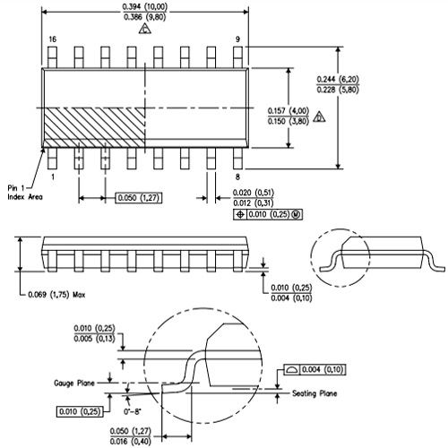
2D Model and Dimensions
Below is the 2D model of the decoder IC, along with its dimensions in inches(millimeters). The following information can be used in order to create custom footprints that can be used for PCB designing and CAD modelling.