RB-156 - Bridge Rectifier
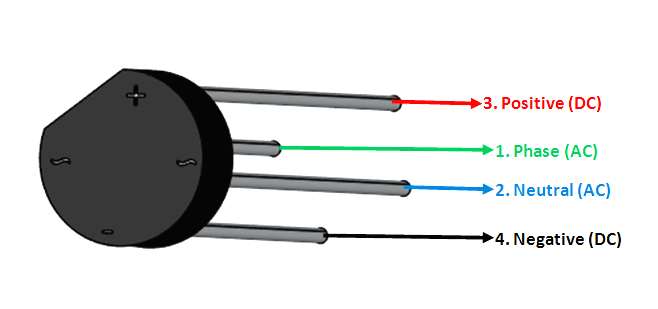
RB-156 Pin Configuration
|
Pin Number |
Pin Name |
Type |
Description |
|
1 |
Phase / Line |
AC Input |
The Phase (Line/Hot) wire from the AC supply is connected to this pin. |
|
2 |
Neutral |
AC Input |
The Neutral Wire from the AC supply voltage is connected to this pin |
|
3 |
Positive |
DC Output |
The rectifier Positive DC voltage can be received from this pin |
|
4 |
Negative /Ground |
DC Output |
The rectifier ground voltage (Negative) can be obtained from this pin. |
RB156 Technical Specifications
The RB-15 series of Bridge rectifiers have many sub categories like RB151 to RB158. Out of which the RB156 is commonly used one and the specification of the same is given below.
- Single Phase low cost Bridge Rectifier
- Maximum Input Voltage (VRMS): 560V
- Maximum Peak Reverse Voltage (VRRM): 800V
- Output DC Current: 1.5A (max)
- Voltage Drop Per Bridge: 1V @ 1A
- Output Voltage: (√2×VRMS) – 2 Volt
- Surge current: 50A
Note: Complete technical information can be found in the RB-156 Datasheet linked at the bottom of this page.
RB-156 Equivalents
W08
Other Bridge Rectifier Packages
DB107S, W-Series (W01 – W10), KBPC2510, GBU1008, AM154
Where to Use RB-156 Bridge Rectifier
The RB-156 is a commonly used Single Phase, compact and low cost Bridge rectifier package. The maximum input AC voltage of this IC is 560V hence can be used in all countries for single phase mains supply. The maximum DC current that this IC can provide is 1.5A. So if you are looking for an IC which can convert AC to DC and supply upto 1.5A for your project, then this IC might be the right choice for you.
How to use RB-156
Using the RB-156 is relatively simple. As the name suggests, the IC just has a full bridge rectifier inside it, which is nothing but four diodes as below.
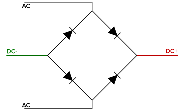
The Four pins (AC,AC,DC-,DC+) are pulled out as four pins as shown in the pin out diagram. We just have to connect the AC supply to the AC pins and the rectified DC voltage will be obtained from the DC+/DC- pins. As simple as it might sound, might there are some design factor that are to be considered while implementing a AC to DC converter which will not be discussed much here.
The output DC voltage of the IC can be calculated using the formulae-
DC Out = (√2×VRMS) – 2 Volts
Where VRMS is the input RMS voltage and -2 is for the voltage drop that appears across each diode path during rectification.
Another important component without which this component cannot be used is the electrolytic capacitor or in this case it is called a smoothing capacitor. The DC output coming from this IC is not a pure DC wave; it has to be smoothed with the help of capacitors. The below GIF will help you to understand the process much better.
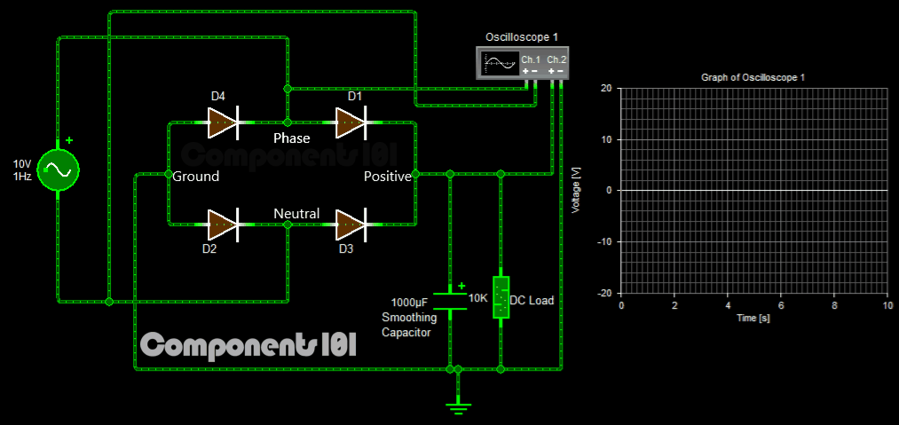
In this GIF, the Diodes D1,D2,D3 and D4 forms the full bridge rectifiers which is present inside out RB-156 IC. A smoothing capacitor of 1000uF is used and a 10K resistor is used as a DC load. As the working of a full bridge rectifier states you can notice that only two diodes will conduct at any given time and thus rectifies the AC to DC. You can also note the Graph being plotted for the Input AC voltage as Red Color and the output DC voltage as Blue colour.
Applications
- AC to DC converter circuits
- Consumer electronics
- Rectifier circuits
- Battery Chargers
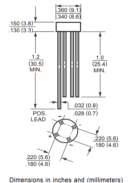
2D – Model