AHV85003 and AHV85043 isolated SiC gate driver chipsets are optimized for driving discrete SiC FETs
Different Types of IC Packages and How to Select One
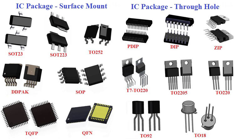
From bulky vacuum tubes to compact SMD ICs, there has been a lot of transition in the way electronics components appeared or packaged. Manufacturers are constantly working to shrink the size of ICs, and furthermore, multiple components are also being gradually integrated into LSI, VLSI, and ULSI designs to reduce the number of components on board. Today almost all components are available in two or more different types of packages among which the engineer can select the one which suits his application best. In this article, we will learn about the different IC package types and where they can be useful.
IC Fabrication
Before we dive into the different types of IC packages, let's quickly learn about the IC fabrication process. As a matter of fact, ICs consist of monolithic, hybrid, or film circuits. The IC manufacturing Steps are as follows-
1. Lithography - It is a process to define a pattern wherein a photoresist material is uniformly applied on the wafer surface and then baked to harden. Later, light is projected through a reticle containing mask information and it is selectively removed.
2. Etching - The unwanted materials are removed from the surface of the wafer.
3. Deposition - By the method of Physical Vapor deposition and chemical vapor deposition, materials are applied on the wafer.
4. Chemical Mechanical Polishing - A planarization technique by applying a chemical slurry with etchant agents to the wafer surface.
5. Oxidation: In the oxidation process, oxygen (dry oxidation) or H O (wet oxidation) molecules convert silicon layers on top of the wafer to silicon dioxide.
6. Ion Implantation: The most widely used technique to introduce dopant impurities into the semiconductor. The ionized particles are accelerated through an electrical field and targeted at the semiconductor wafer.
7. Diffusion: A diffusion step following ion implantation is used to anneal bombardment-induced lattice defects.
IC Package Types
The packages are classified into two kinds on the basis of how they are mounted on a circuit board.
Through-Hole Mount Packages
They are designed in a way that the lead pins are stuck through one side of the board and soldered on the other. They are bigger in size as compared to the other kind. These are majorly used in electronic equipment to compensate for the board space and cost limitations. Dual inline packages are one of the examples of through-hole mount packages.
To add on to that classification, Through-hole mount packages come in ceramic and plastic types.
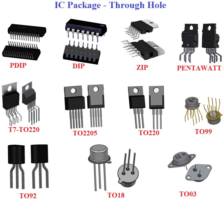 These are the most significantly used IC packages is Dual Inline Packages (DIP). Just like in 28-pin ATmega328, the pins are placed in parallel to each other extending perpendicularly and laid out on a black plastic housing which is rectangular in shape. The pins are spaced at 0.1 inches.
Furthermore, the package varies in size due to the difference in the number of pins in different packages. The number ranges from 4 to 64. These pins are placed in a manner that they can be adjusted on to the center of a breadboard without short-circuiting each other or even get smoldered into PCBs.
There are many types of DIP Packages, Plastic Dual In-Line Package (PDIP) and Molded Dual In-Line Package (MDIP) are the few popular types. Further, it can be classified as-
Standard - This is the most common packaging. The pins are spaced 0.1” apart.
Skinny - In this packaging, the space between the terminal rows is 7.62mm.
Shrink - Similar to the standard ones but the lead pitch is 1.778 mm. Smaller in size, they use high pin density packaging.
Zig-Zag in Line Packages (ZIP)- The pins in this kind of a package are inserted perpendicularly to the circuit board. These pins are perpendicularly aligned in the package and closer to each other. This sort of packaging was short-lived and was mainly used in dynamic RAM chips. Other types of through holed packages include CER-DIP in which the lead pitch is 2.54mm and the body is molded with ceramics. Also, the sealing material used in this is glass. Pin Grid Array (PGA) in the lead pitch is 2.54 mm, and the body is made out of ceramics. The pins are arranged vertically from the body and can be placed on a grid. This one usually suits a multi-pin packaging.
Surface Mount Packaging
Surface mount packaging follows the technology of mounting or placing the components directly on the printed circuit board surface. Although this process of fabrication helps do things quickly, it also increases the chances of defects. This is because of the miniaturization of components and also because they are mounted extremely close to each other. This, in turn, results in making it extremely important to detect the failure in the entire process. Again, Surface mount packaging also uses ceramic or plastic molding.
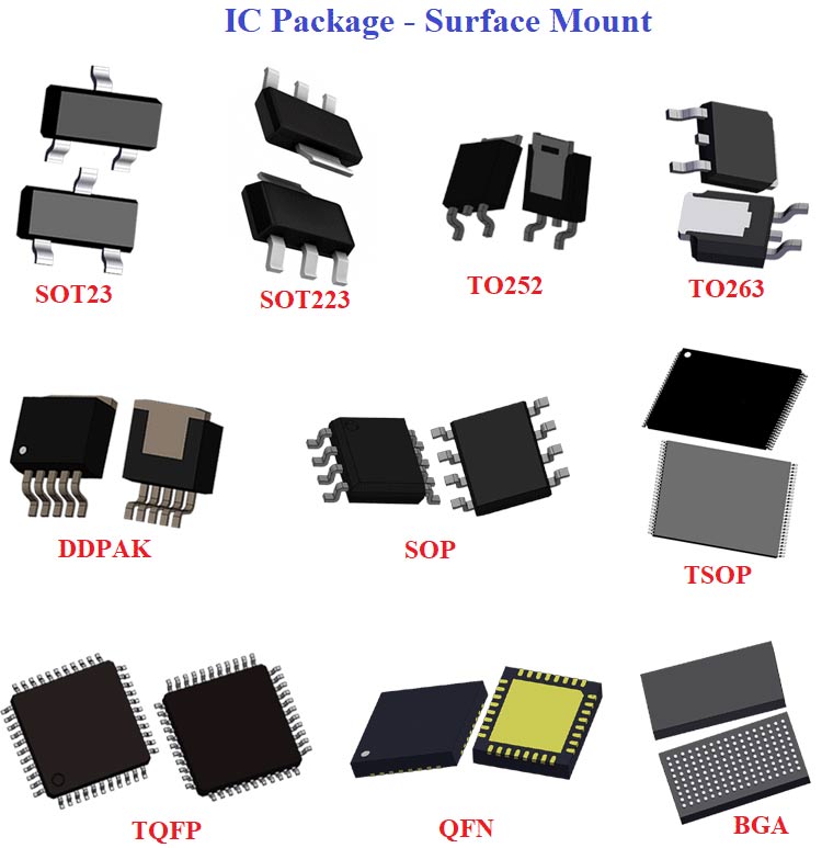
The different types of surface mount packages that use plastic molds are as following-
Small outline L-leaded package- This type has gull-wing type leads that draw out on either direction from the body in an L fashion and can be mounted directly on the board.
Quad Flat L-leaded Packages (QFP)- These are similar to SOP. However, the only difference is that the leads are drawn out in 4 directions instead of 2 and are mounted directly on the board. They also come with a heat sink and built-in heat spreader.
Ball Grid Array (BGA) - These have solder ball arrays on the back surface of PCBs.
Fine Pitch Land Grid Array- These have solder land arrays on the back surface of PCBs.
Wafer Level Chip Size Package- Many Individual chips are made out of a packaged wafer that is cut out.
Through Hole Mounting VS Surface Mounting
The two packaging types - mainly through-hole mounting and surface mounting have their individual perks and disadvantages. Here’s a comparison between through-hole and surface mount devices with various factors that alter the need for the type of IC packages.
1. Size - Surface mount packages are smaller in comparison to through-hole packages.
2. Component density - Surface mounting packages have a comparatively higher component density as well as the density of connections.
3. Assembling- Tiny errors are automatically corrected by the molten solders that pull components close together due to tension in surface mounting packages, unlike through-hole packages that cannot afford even the slightest of errors while making holes. This is because the alignment, once made, cannot be corrected.
4. Electromagnetic compatibility - It is the ability of different electronic devices and components to work correctly even in the presence of other devices that emit electromagnetic waves. Surface mounting packages have a better EMC performance.
5. Cost - The cost of production is also lower than that of through-hole packages because of automated methods.
However, Surface mount packages cannot function along with a simple plugin on the breadboard. They require to be mounted upon a pin-led carrier. Or worse even, they may need special PCBs customized to different prototypes separately.
Selecting the Right IC Package for your Application
First things first, let us stress enough on how important it is to have good packaging. Integrated circuits are put into packages to facilitate smooth handling and assembly on the printed circuit boards. It is extremely imperative to put ICs into packages in order to avoid any kind of damage and corrosion. Also, the packages help in dissipating the heat produced. However, this is the final part of the entire process of fabrication. Before deciding on the kind of packaging that best suits you, look into certain important factors such as - assembly capability, power, cost, and connectivity.
With the ever going developments, there have emerged many kinds of packages for Semiconductor Integrated Circuits. The motive is to choose the right kind of IC package for yourself which is affordable and still not compromise with the performance.


