TOP248YN AC-DC Off-Line Switcher
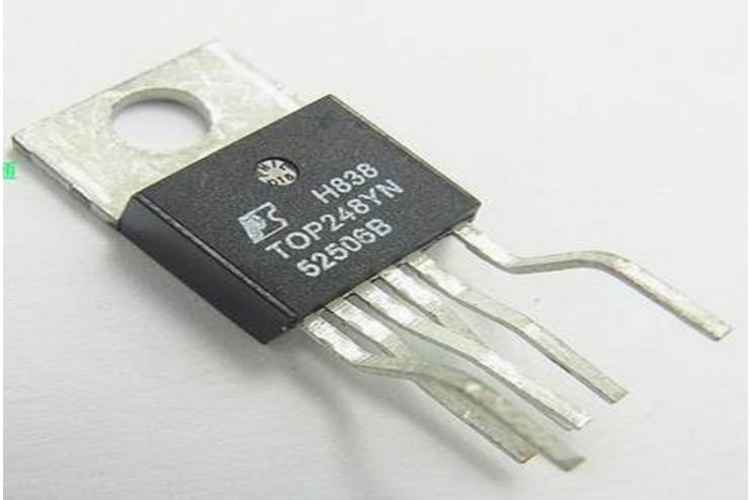
The TOP248 is a highly integrated, monolithic off-line switcher IC designed for use in low-power offline flyback converters. Manufactured by Power Integrations, it incorporates a 700 V power MOSFET, high-voltage switched current source, and current-mode PWM control circuitry into a single chip. The TOP248 can operate without a heat sink for applications up to 34 W when using P/G packages, contributing to cost savings and system simplification. Its integrated features minimize or eliminate the need for external components, further reducing overall costs. The inclusion of a fully integrated soft-start ensures minimal stress and overshoot during startup, while an externally programmable accurate current limit enhances precision and flexibility. With a wider duty cycle, it enables higher power output with smaller input capacitors, optimizing space utilization. The TOP248's separate line sense and current limit pins, along with various protections like UV and OV shutdown, ensure robust performance under various conditions, including line surges. Its EcoSmart technology enhances energy efficiency with extremely low consumption in remote off mode and frequency adjustment for high standby efficiency. Additionally, its frequency jittering feature reduces EMI, while thermal management features like hysteretic thermal shutdown and large thermal hysteresis enhance reliability and prevent overheating.
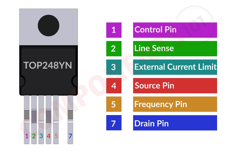
TOP248 Pinout Configuration
Here we have only included the pinout details for the TO-220-7C, TO-262-7C and TO-263-7C packages. For DIP-8B and SMD-8B packages, the pinout is different. Please refer to the datasheet attached at the end of this page, for details about these packages.
| NAME | PIN | DESCRIPTION |
| Control Pin | 1 | Error amplifier and feedback current input pin for duty cycle control. |
| Line Sense | 2 | Input pin for OV, UV, line feed forward with DCMAX reduction, remote ON/OFF and synchronization. A connection to the SOURCE pin disables all functions on this pin. |
| External Current Limit | 3 | Input pin for external current limit adjustment, remote ON/OFF, and synchronisation. A connection to the SOURCE pin disables all functions on this pin. |
| Source Pin | 4 | Output MOSFET source connection for high voltage power return. Primary side control circuit common and reference point. |
| Frequency Pin | 5 | Input pin for selecting switching frequency: 132 kHz if connected to the SOURCE pin and 66 kHz if connected to CONTROL pin. The switching frequency is internally set for fixed 132 kHz operation in P and G packages. |
| Drain Pin | 7 | High voltage power MOSFET drain output. |
Features
- Extended Power Range Soft-Start
- Under-Voltage Detection
- Over-Voltage Shutdown
- Externally Programmable Current Limit
- Wider Duty Cycle
- Frequency Jitter
- Separate Line Sense and Current Limit Pins on Y Package
- Line Feed Forward
- 132/66 KHz Operation
- Hysteretic Thermal Shutdown
- Remote ON/OFF
- Half Frequency Option in Y Package
- Standard Packages with Omitted Pins for Large Creepage
How to Identify the TOP248 Part Number
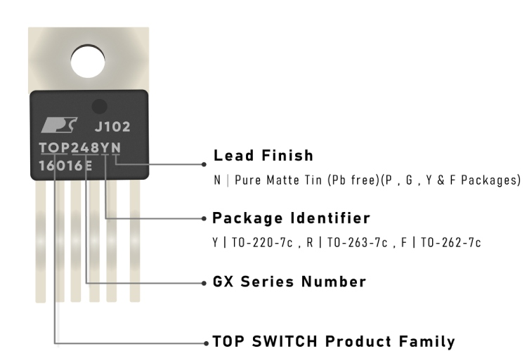
The TOP248 is available in different packages. You can identify them using the package marking. You can use the above image to identify the TOP248 packages. TOP indicates the TOP Switch product family while the next 3 digits (for example 248) indicate the product series. The next alphabet indicates the package, G for SMD-8B (TOP242-246 only), P for DIP-8B (both TOP242-246 only), Y for TO-220-7C, R for TO-263-7C and F for TO-262-7C packages. The next alphabet denotes the lead finish, if it's N it indicates lead-free and for leaded this is left blank.
Manufacturers of TOP248YN:
The TOP248 is manufactured by Power Integrations, under their TOP Switch-GX series of ICs. There are no alternative manufacturers for the same part number as of the date of writing this article.
TOP248YN Equivalents
If you are looking for an equivalent or replacement for TOP248 you can look at the other ICs from the same family. The only difference between them will be the maximum power rating. You can use the following table to select a proper one.
| Product | 230 VAC ±15% | 85-265 VAC | ||
| Adapter | Open Frame | Adapter | Open Frame | |
| TOP242 P or G TOP242 R TOP242 Y or F |
9 W 15 W 10 W |
15 W 22 W 22 W |
6.5 W 11 W 7 W |
10 W 14 W 14 W |
| TOP243 P or G TOP243 R TOP243 Y or F |
13 W 29 W 20 W |
25 W 45 W 45 W |
9 W 17 W 15 W |
15 W 23 W 30 W |
| TOP244 P or G TOP244 R TOP244 Y or F |
16 W 34 W 30 W |
28 W 50 W 65 W |
11 W 20 W 20 W |
20 W 28 W 45 W |
| TOP245 P or G TOP245 R TOP245 Y or F |
19 W 37 W 40 W |
30 W 57 W 85 W |
13 W 23 W 26 W |
22 W 33 W 60 W |
|
TOP246 P or G TOP246 R |
21 W 40 W |
34 W 64 W |
15 W 26 W |
26 W 38 W |
| TOP247 R TOP247 Y or F |
42 W 85 W |
70 W 165 W |
28 W 55 W |
43 W 125 W |
| TOP248 R TOP248 Y or F |
43 W 105 W |
75 W 205 W |
30 W 70 W |
48 W 155 W |
| TOP249 R TOP249 Y or F |
44 W 120 W |
79 W 250 W |
31 W 80 W |
53 W 180 W |
| TOP250 R TOP250 Y or F |
45 W 135 W |
82 W 290 W |
32 W 90W |
55 W 210W |
TOP248YN Alternatives
UC3843, UC3844, LM5022, LM5023, LM5026
Note: Complete technical details can be found in the TOP248YN datasheet at this page’s end.
TOP248YN Schematics
The following image shows the typical TOP248YN circuit diagram.
As you can see the circuit is very simple and only requires bare minimum components. No need for any switching elements and the feedback is done using an optocoupler. The circuit shown below is for a low-cost, high-efficiency, 7 W (10 W peak) Multiple Output Flyback Converter for DVD Applications with Primary Sensed Feedback.
The AC input goes through the fuse and then a common mode chock to the bridge rectifier. The rectified output is then fed to the primary side where it is switched using the TOP248PN. The resistor R4 is used to set the undervoltage and overvoltage limits. The output side contains the rectifier and filter circuits for the 12V output. The output voltage is regulated by the help of a Zener diode in combination with an optocoupler. The optocoupler uses the control pin on the TOP248 to regulate the output.
Design Tips for TOP248YN
● What's the maximum power that we can get from a TOP248YN SMPS?
From an open frame power supply built around a TOP248YN, we can get up to 205W power for a fixed 230 VAC input and 155W for universal input (85-265 VAC). From an adapter-type or closed power supply, we can get 105W power for the fixed input voltage of 230 VAC and 70W for universal input (85 -265 VAC).
● What is the maximum output current supported by the TOP248YN?
The TOP248YN can support maximum output currents typically up to around 3A, depending on the specific design and application requirements.
● What protections are built into the TOP248YN?
The TOP248YN includes various built-in protections such as overtemperature, overvoltage, and overcurrent protections, enhancing the reliability and safety of the power supply it is used in.
● Can the TOP248YN operate in a constant voltage (CV) mode?
Yes, the TOP248YN can operate in both constant voltage (CV) and constant current (CC) modes, making it suitable for various applications requiring different output characteristics.
● What is the typical switching frequency of the TOP248YN?
The TOP248YN typically operates at a switching frequency of around 132 kHz, which helps in reducing the size of transformers and power supplies while maintaining efficiency.
● Do we need an external MOSFET with TOP248YN?
No, we don’t. The TOP248YN feature an integrated power MOSFET.
● What are the design considerations when designing an TOP248 power supply PCB?
When designing a board for the TOP248-based power supply, adhere to the following guidelines:
- Single Point Grounding: Implement a single point (Kelvin) connection at the negative terminal of the input filter capacitor for the TOP248 SOURCE pin and bias winding return. This enhances surge capabilities by directing surge currents directly to the input filter capacitor.
- Control Pin Bypass Capacitor: Place the CONTROL pin bypass capacitor as close as possible to the SOURCE and CONTROL pins. Ensure that the SOURCE connection trace is not shared by the main MOSFET switching currents. Components connected to the MULTIFUNCTION, LINE-SENSE, or EXTERNAL CURRENT LIMIT pins should also be located closely between their respective pin and SOURCE. Separate traces for SOURCE pin switching currents are critical due to its function as the controller ground reference pin.
- Minimize Trace Lengths: Keep traces to the M, L, or X pins short and away from the DRAIN trace to prevent noise coupling. Locate the LINE-SENSE resistor close to the M or L pin to minimize trace length.
- Feedback Optocoupler Placement: Position the feedback optocoupler output close to the CONTROL and SOURCE pins of the TOP248 for optimal performance.
- Y-Capacitor Connection: Connect the Y-capacitor close to the secondary output return pin(s) and the positive primary DC input pin of the transformer.
- Heat Sinking: For Y package (TO-220) or F package (TO-262), avoid electrically tying the heat sink tab to any primary ground/source nodes on the PCB to prevent circulating currents. In P (DIP-8), G (SMD-8), or R (TO-263) packages, use a copper area underneath the package connected to the SOURCE pins as an effective heat sink. Utilize both top and bottom side areas connected with vias on double-sided boards to increase effective heat sinking area. Additionally, provide sufficient copper area at the anode and cathode leads of the output diode(s) for heat sinking.
Troubleshooting Tips for TOP248YN
Here are some troubleshooting tips for dealing with issues related to the TOP248YN:
● No Output Voltage or Power Supply Not Starting:
Ensure the input power is connected and within the specified range for the TOP248.
Check for a blown fuse or faulty rectifier diode, which can prevent the circuit from powering up.
Double-check all component values, especially feedback resistors, to ensure they are within the specified range.
● Overheating or Thermal Shutdown:
Ensure sufficient cooling for the TOP248. Overheating can result from inadequate heat sinking or poor airflow.
Avoid overloading the power supply, as excessive heat can be caused by overloading. Ensure the load is within the IC's specified limits.
Look for potential short circuits on the output side that might cause excessive current draw.
● Unstable Output Voltage:
Verify that the feedback loop is correctly designed, and components are not defective. Incorrect feedback can lead to unstable output.
Check for low-quality or degraded capacitors, as they can cause instability. Ensure capacitors with low ESR values are used.
● Excessive Noise or Ripple:
Ensure that input and output filter capacitors are of adequate value and quality to minimize noise.
Address any layout issues, as poor PCB layout can contribute to noise. Minimize trace lengths and properly route high-current paths.
● Underperformance in Load Regulation:
Confirm that the load is within the TOP248's capabilities to ensure proper load regulation.
Verify the values of feedback resistors, as incorrect values can affect load regulation.
● Electromagnetic Interference (EMI) Issues:
Follow good PCB layout practices to minimize EMI.
Implement proper shielding and grounding techniques to reduce EMI.
● Unexpected Resets or Shutdowns:
Check for transient voltage spikes using an oscilloscope, as they can cause resets. Ensure that the circuit is adequately protected against such spikes.
Monitor the temperature of the TOP248 to ensure it is within the rated temperature range using non-contact thermometers or thermal cameras.
Applications
- LCD monitors
- Personal computers
- Small servers
- Laptop adapters
- Set-top boxes.
- Digital TVs
- Printers
- DVD Players and Recorders
- UPS
- Video Games
- Broadband Modems
- Cellular phone adapters
- Audio Amplifiers
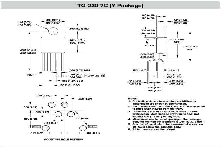
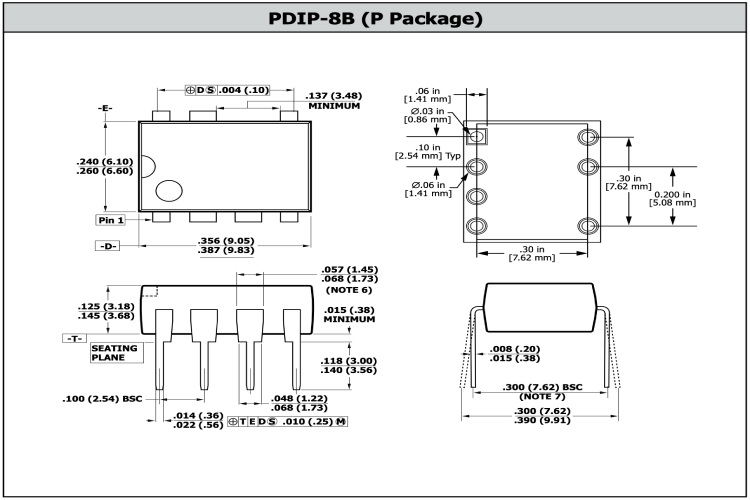
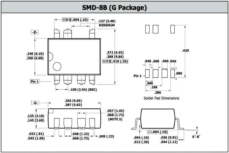
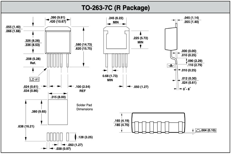
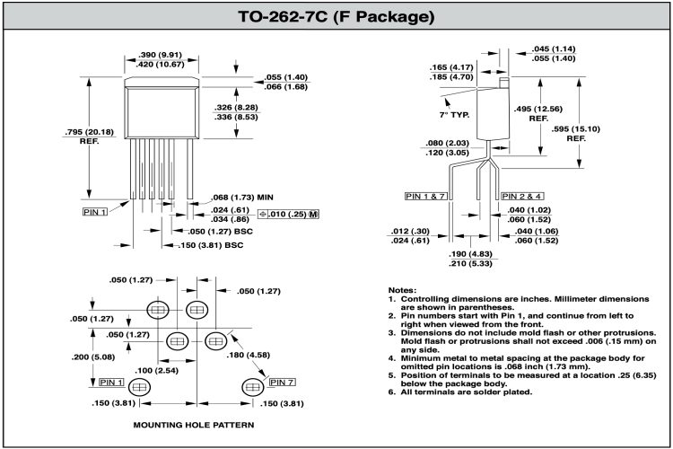
2D-Model and Dimensions
Below is the 2D CAD drawing of TOP248YN along with its dimensions. The dimensions can be used to create custom footprints of the module and be used for PCB or CAD modelling. We have also included 2D CAD drawings for other packages that TOP248 is available.