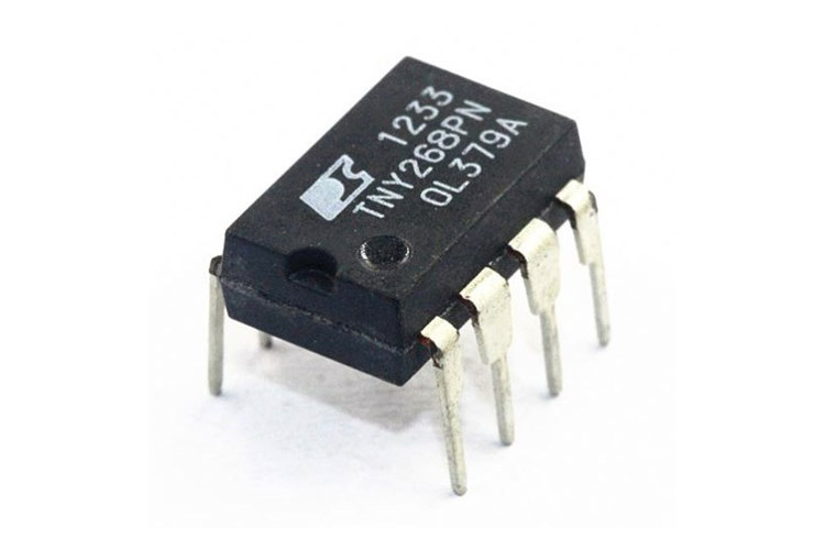
TNY268PN Enhanced, Energy Efficient, Low Power Off-line Switcher
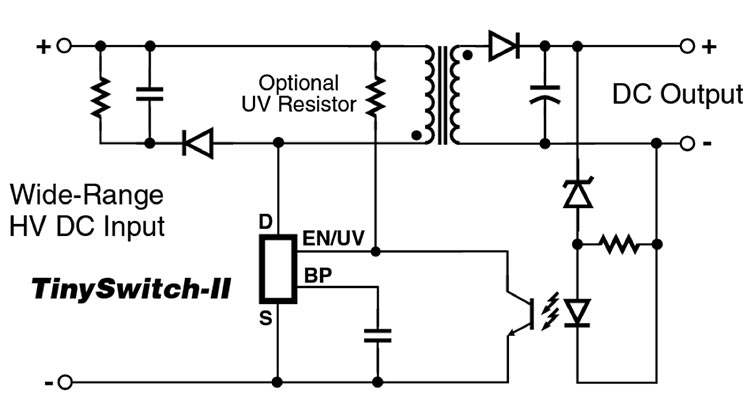
The TNY268PN IC belongs to the TNY26x series of ICs, it is manufactured by Power Integrations along with other Power-switching ICs under its TinySwitch collection. The TNY26x series ICs are designed for high-efficiency power supply applications, integrating a PWM controller and a power MOSFET into a single monolithic component. These ICs operate under a wide input voltage range, making them versatile for various applications. The series features an innovative energy-saving technology that reduces power consumption under light-load or no-load conditions. It also includes multiple protection features such as over-temperature, over-current, and output short-circuit protection, enhancing system reliability. The TNY26x series is optimized for compact designs, reducing the need for external components, and simplifying circuit layout, particularly beneficial in space-constrained applications.
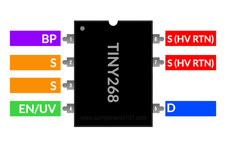
TNY268 Pinout Configuration
|
PIN |
SYMBOL |
DESCRIPTION |
| 1 | BP |
Connection point for a 0.1 µF external bypass capacitor for the internally generated 5.8 V supply |
| 2 | S |
Control circuit common, internally connected to output MOSFET source. |
| 3 | S |
Control circuit common, internally connected to output MOSFET source. |
| 4 | EN/UV |
enable input and line under-voltage sense. |
| 5 | D |
Power MOSFET drain connection. |
| 7 | S (HV RTN) |
Output MOSFET source connection for high voltage return |
| 8 | S (HV RTN) |
Output MOSFET source connection for high voltage return |
TNY26x TinySwitch-II Variants
Within the TNY26X series, there are multiple parts available. Each variant has a different power handling capacity. Here are the available chip variants with their rated output power.
| OUTPUT POWER TABLE | ||||
| PRODUCT |
230 VAC ±15% |
85-265 VAC |
||
| ADAPTER | OPEN FRAME | ADAPTER | OPEN FRAME | |
|
TNY263 P or G |
5 W | 7.5 W | 3.7 W | 4.7 W |
|
TNY264 P or G |
5.5 W | 9 W | 4 W | 6 W |
|
TNY265 P or G |
8.5 W | 11 W | 5.5 W | 7.5 W |
|
TNY266 P or G |
10 W | 15 W | 6 W | 9.5 W |
|
TNY267 P or G |
13 W | 19 W | 8 W | 12 W |
|
TNY268 P or G |
16 W | 23 W | 10 W | 15 W |
Features of TNY268PN
- Reduced System Cost
- Fully integrated auto-restart for short circuit and open loop fault protection – saves external component costs.
- Built-in circuitry practically eliminates audible noise with ordinary dip-varnished transformer.
- Programmable line under-voltage detect feature prevents power on/off glitches – saves external components.
- Frequency jittering dramatically reduces EMI (~10 dB) – minimizes EMI filter component costs.
- 132 kHz operation reduces transformer size – allows use of EF12.6 or EE13 cores for low cost and small size.
- Very tight tolerances and negligible temperature variation on key parameters eases design and lowers cost.
- Lowest component count switcher solution
- Expanded scalable device family for low system cost.
- Better Cost/Performance over RCC & Linears.
- Lower system cost than RCC, discrete PWM and other integrated/hybrid solutions
- Cost effective replacement for bulky regulated linears.
- Simple ON/OFF control – no loop compensation needed.
- No bias winding – simpler, lower cost transformer
- Simple design practically eliminates rework in manufacturing.
- EcoSmart – Extremely Energy Efficient
- No load consumption <50 mW with bias winding and <250 mW without bias winding at 265 VAC input
- Meets California Energy Commission (CEC), Energy Star, and EU requirements.
- Ideal for cell-phone charger and PC standby applications High Performance at Low Cost
- High voltage powered – ideal for charger applications.
- High bandwidth provides fast turn on with no overshoot.
- Current limit operation rejects line frequency ripple.
- Built-in current limit and thermal protection improves Safety.
TNY268PN Equivalent
TNY278, NCP1014, LNK304, LNK306, NCP1702,
Note: Complete technical details can be found in the TNY268PN datasheet at this page’s end.
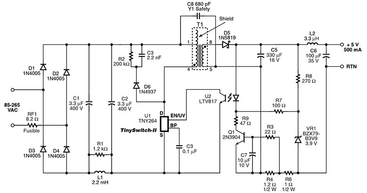
TNY268PN Circuit Diagram
Image below shows the typical schematic diagram for TNY268 offline switcher.
The circuit below is for a 2.5W constant voltage constant current power supply with universal input. The primary side contains the PMIC itself along with the rectifier circuit, protection circuit and the capacitive dropper for the PMIC. In the secondary side we have ethe feed circuit for the voltage and current control along with output rectifier and filter circuit.
TNY268PN Applications
- Low power adapters/chargers for cell phones, PDAs, digital cameras, portable audio/video players, and power tools
- Standby for PCs and TVs
- Embedded power supplies for DVD players/recorders, set-top boxes, and home appliances.
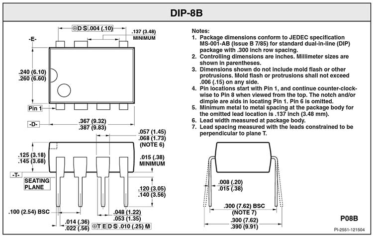
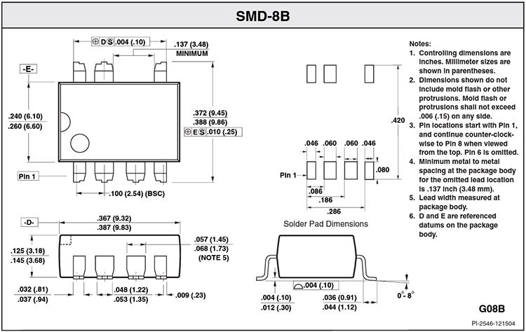
2D-Model and Dimensions
Below is the 2D CAD drawing of TNY268PN IC along with its dimensions in millimetres. The dimensions can be used to create custom footprints of the module and be used for PCB or CAD modelling. Here we have only given the dimensions for SO8 package. Please reference the datasheet for details on other packages.
You can find the TNY268PN datasheet pdf along with application circuit and price below.


