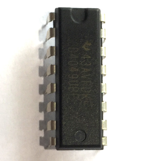
4049 Hex Inverter Buffer IC
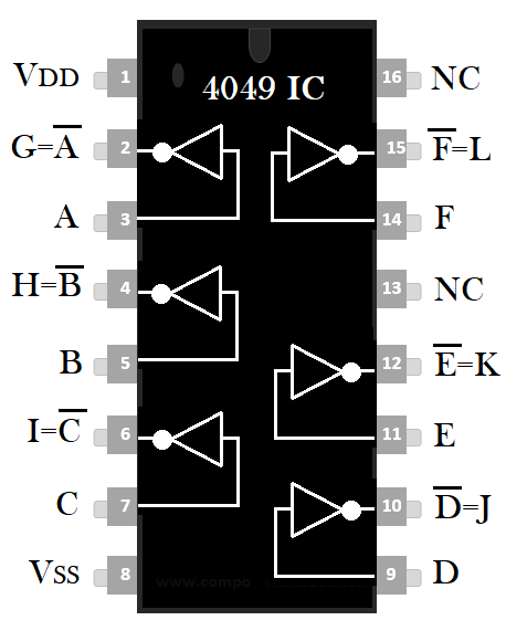
4049 Pin Configuration
|
Pin Number |
Pin Name |
I/O |
Description |
|
1 |
VDD |
- |
Positive supply for IC |
|
2 |
G |
O |
Inverting output 1 for input 1 |
|
3 |
A |
I |
Input 1 |
|
4 |
H |
O |
Inverting output 2 for input 2 |
|
5 |
B |
I |
Input 2 |
|
6 |
I |
O |
Inverting output 3 for input 3 |
|
7 |
C |
I |
Input 3 |
|
8 |
VSS |
- |
Negative supply for IC |
|
9 |
D |
I |
Input 4 |
|
10 |
J |
O |
Inverting output 4 for input 4 |
|
11 |
E |
I |
Input 5 |
|
12 |
K |
O |
Inverting output 5 for input 5 |
|
13 |
NC |
- |
Not connected |
|
14 |
F |
I |
Input 6 |
|
15 |
L |
O |
Inverting output 6 for input 6 |
|
16 |
NC |
- |
Not connected |
Features
- Mostly used in voltage multiplier circuit
- Accept High input supply voltage
- Used to low the high logic levels
- High sink current for driving two TTL loads
- Special input protection allows input voltages greater than VDD
- 100% Tested for Quiescent Current at 20 V
- Available packages: PDIP, SOIC, TSSOP, SO with 16 number of pins
- Maximum input current of 1uA at 18v over full package temperature range
- Compatible in use with breadboard and perf board
Technical Specification
- Input supply voltage ranges from 3v (min.) to 18v (max.)
- Supply current 50mA (max.)
- Ambient Temperature ranges from -40 to +85°C
- Input capacitance is 22.5pf (max.)
- As input voltage increase from 5v to 15v, output current sink also vary from 1.8 to 26mA
Note: Complete technical information can be found in the 4049 Datasheet linked at the bottom of this page.
4049 Equivalent ICs
74LS04, SG3525
Similar IC
HEF4049B, CD4050B
Brief Description
The IC 4049 consists of six NOT gate inside it and having a high input supply voltage with a maximum current rating of 1mA at 18v. 4049 IC is capable to drive two TTL loads. The main use of this IC is to create a voltage multiplier circuit by simply adding resistor, capacitor, and diode with it. It also used for the conversion of high logic levels to low. Also you can drive two TTL loads with it. The operating temperature of the IC is -40 to +85 °C. The IC is having high current sink as the input voltage the increase the output current sink value will increase, at 15v the current sink value is 26mA.
Where to use?
4049 IC used for many applications; basically it help in creating voltage multiplier circuit and also one can create a square wave oscillator circuit through it. The IC is also useful in getting inverting output as it contains NOT gate inside it. It can also be useful in making various projects like simple LED torch light, Automatic Street light, magic eye, and automatic guest detector at home door.
How to use?
We can use this IC to make a square wave oscillator with less energy consumption. The square wave oscillator circuit consist one resistor and capacitor and 4049 IC with it. The frequency determined by the resistor R1 and capacitor C1 can be obtained by the formula below:
F = 1 / (1.39 * R1 * C1)
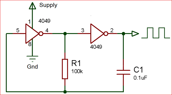
The supply voltage to be used in the circuit have ranged from 3v to 12v of DC voltage. It’s easy to make and you will get the square wave output at the output pin.
Applications
- Voltage multiplier circuit
- High to low logic converter
- CMOS hex buffer
- Source driver
- CMOS to TTL/DTL Hex converter
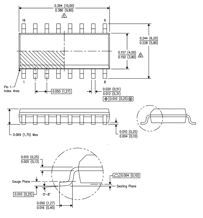
2D-Model and Dimensions
The 2D dimension will help you in using this IC on breadboard or perf board.