TIP125 PNP Darlington Transistor Pinout, Specifications, Working & Datasheet Guide
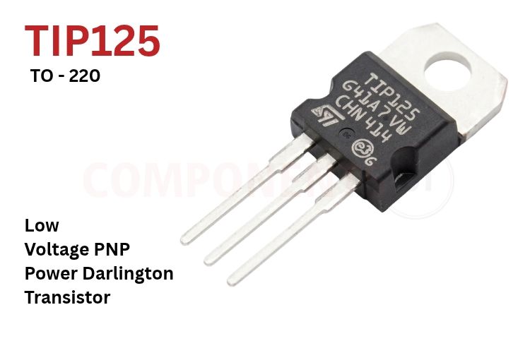
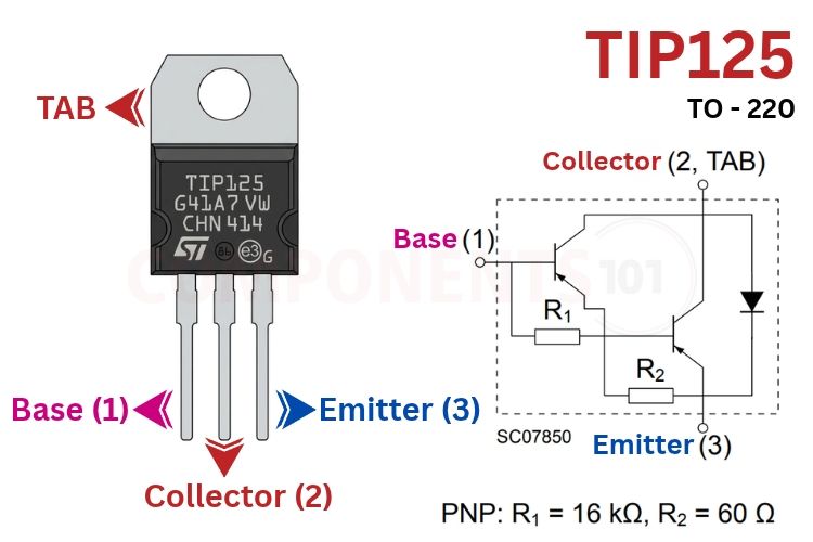
The TIP125 is an epitaxial-based PNP silicon power transistor configured in a monolithic Darlington pair and housed in the through-hole TO-220 plastic package. The TIP125 is engineered specifically for general-purpose medium-power linear amplification and low-speed power switching applications. It offers a maximum collector-emitter voltage rating of -60V (VCEO), a continuous collector current rating of -5.0 A (IC), and a high DC gain (hFE) of at least 1000 at -3.0 A.
TIP125 Pinout Configuration
The TIP125 follows the standard JEDEC TO-220 pinout shared across the TIP120/TIP125 series. Looking at the front marked face with the three leads pointing downward.
| Pin Number | Pin Name | Terminal Type | Function & Description |
| 1 | Base (B) | Control Input | Controls the conduction state of the Darlington pair. Current is drawn out of the base to turn the transistor ON. |
| 2 | Collector (C) | Power Output | Main power output terminal connected to the load. Internally bonded directly to the metal mounting tab. |
| 3 | Emitter (E) | Power Supply | Common emitter terminal connected to the positive DC power supply rail (+VCC) in standard high-side switching circuits. |
| Tab | Collector (C) | Thermal Tab | Metallic mounting tab for heatsink attachment. Electrically continuous with Pin 2 Collector. |
TIP125 Transistor Features and Specifications
●High DC current gain: hFE = 1000 minimum (typical 1000 to 5000) at IC = -3.0 A, VCE = -3.0 V
●Continuous collector current capability: IC = -5.0 A
●Peak pulsed collector current rating: ICM = -8.0 A
●Maximum collector-emitter breakdown voltage: VCEO = -60V (with base open, IB = 0)
●Maximum collector-base breakdown voltage: VCBO = -60V (with emitter open, IE = 0)
●Maximum emitter-base reverse breakdown voltage: VEBO = -5.0V (with collector open, IC = 0)
●Maximum base drive current: IB = -0.12 A (120 mA)
●Low base drive requirement: Less than 5 mA to 12 mA needed to saturate heavy 3A to 5A loads
●Total power dissipation: PTOT = 65W at case temperature TC ≤ 25°C (derated linearly at 0.52 W/°C above 25°C)
●Total power dissipation in free air: PTOT = 2.0W at ambient temperature TA ≤ 25°C
●Integrated internal base-emitter bleed resistors: R1 = 16 kΩ across Q1 base-emitter, R2 = 60 Ω across Q2 base-emitter.
| Electrical Parameter | Symbol | Test Conditions | Minimum | Maximum | Unit |
| Collector-Emitter Sustaining Voltage | VCEO(sus) | IC = -30 mA, IB = 0 | -60 | - | V |
| Collector Cut-off Current | ICEO | VCE = -30 V, IB = 0 | - | -0.5 | mA |
| Collector Cut-off Current | ICBO | VCB = -60 V, IE = 0 | - | -0.2 | mA |
| Emitter Cut-off Current | IEBO | VEB = -5.0 V, IC = 0 | - | -2.0 | mA |
| Collector-Emitter Saturation Voltage | VCE(sat) | IC = -3.0 A, IB = -12 mA | - | -2.0 | V |
| Collector-Emitter Saturation Voltage | VCE(sat) | IC = -5.0 A, IB = -20 mA | - | -4.0 | V |
| Base-Emitter On Voltage | VBE(on) | IC = -3.0 A, VCE = -3.0 V | - | -2.5 | V |
| DC Current Gain | hFE | IC = -0.5 A, VCE = -3.0 V | 1000 | - | - |
| DC Current Gain | hFE | IC = -3.0 A, VCE = -3.0 V | 1000 | - | - |
| Turn-On Time | ton | IC = -3.0 A, IB1 = -12 mA | - | - | μs |
| Turn-Off Time | toff | IC = -3.0 A, IB1 = -12 mA | - | - | μs |
*Note: Complete Technical Details can be found in the TIP125 datasheet given at the end of this page.
How the TIP125 Darlington Transistor Works
Internal Darlington Working Principle & Architecture
The TIP125 operates as a compound bipolar semiconductor where two PNP transistors (input driver Q1 and main output power transistor Q2) are connected in a classic Darlington topology on a single planar silicon die.
In this cascaded arrangement, the collector terminals of both Q1 and Q2 are joined together to form the external Collector terminal (Pin 2 and Tab). The emitter of driver transistor Q1 feeds directly into the base of power transistor Q2. The base of driver transistor Q1 serves as the external Base terminal (Pin 1), and the emitter of power transistor Q2 serves as the external Emitter terminal (Pin 3).
The overall current gain of the Darlington pair is approximately the product of the individual current gains:
hFE(total) ≈ hFE(Q1) × hFE(Q2)
Because typical small-signal and power PNP transistors provide individual gains between 30 and 80, the composite Darlington configuration yields an effective DC gain exceeding 1000 to 5000. This enables a microcontroller circuit providing only 3 mA to 10 mA of base current to control heavy continuous load currents up to -5.0 A without requiring specialized gate drivers or secondary pre-amplification stages.
Role of Integrated Resistors (R1 and R2)
Discrete high-gain Darlington circuits often suffer from thermal instability and extended turn-off delays due to accumulated minority carrier storage charge. To eliminate these issues, the TIP125 integrates two on-chip diffused resistors:
●Resistor R1 (16 kΩ) is bridged across the base and emitter of driver transistor Q1. It bleeds off high-temperature collector-to-base leakage current (ICBO), preventing accidental thermal turn-on when the base is open or driven from a high-impedance source.
●Resistor R2 (60 Ω) is connected across the base and emitter of output transistor Q2. This low-value resistor provides a fast recombination discharge path for the stored charge inside the wide base region of the power transistor during turn-off, significantly speeding up switching transitions.
Integrated Freewheeling Damper Diode
The TIP125 also includes an integrated anti-parallel diode monolithically diffused between the Collector and Emitter terminals (Anode to Collector, Cathode to Emitter). In inductive switching applications (such as driving relays, solenoids, or small motors), when the transistor turns OFF, the inductive load's magnetic field collapses, generating a reverse voltage transient. The built-in diode helps clamp reverse voltage transients, preventing destructive reverse biasing of the output transistor junctions. For heavy inductive loads drawing over 2A, adding an external Schottky flyback diode (such as 1N5819 or 1N5822) directly across the load terminals remains recommended practice to minimise thermal dissipation inside the transistor package.
Complementary NPN-PNP Pairs (TIP120 Series Family)
The TIP125 belongs to the industry-standard TIP120/TIP125 family of complementary power Darlington transistors. For every PNP variant, an identical NPN counterpart exists with matching electrical parameters, current capacities, and switching dynamics:
| Voltage Rating | NPN Darlington (Low-Side) | PNP Darlington (High-Side) | VCEO Breakdown Rating | Continuous Collector Current (IC) |
| Standard Grade | TIP120 | TIP125 | 60V | 5.0 A |
| Intermediate Grade | TIP121 | TIP126 | 80V | 5.0 A |
| High-Voltage Grade | TIP122 | TIP127 | 100V | 5.0 A |
In complementary Class-AB audio power amplifiers and bidirectional full-bridge (H-bridge) DC motor drivers, pairing the TIP125 with the TIP120 ensures symmetrical rise and fall times, equal saturation characteristics, and minimal crossover distortion across positive and negative power supply rails.
TIP125 Datasheet
The complete manufacturer TIP25 Datasheet provides comprehensive electrical curves including safe operating area (SOA), forward bias DC gain vs. collector current, collector-emitter saturation voltage vs. base current, and transient thermal impedance graphs. For switching designs, focus on VCE(sat) (it sets the heat you must remove), the base current used in the saturation test (12 mA at 3 A), and RθJC/RθJA. For linear designs such as audio stages or pass transistors, the SOA graph is the deciding factor, because the full 65 W is only available at low collector-emitter voltage.
TIP125 Equivalents and Alternative Transistors
When replacing the TIP125 in existing circuits or selecting alternative parts for new designs, consider the following direct and upgraded replacements:
| Part Number | Polarity | VCEO Rating | IC Rating | Package | Compatibility Notes |
| TIP126 | PNP | -80V | -5.0 A | TO-220 | Direct 100% pin-compatible replacement with higher voltage withstand (80V). |
| TIP127 | PNP | -100V | -5.0 A | TO-220 | Universal drop-in replacement with highest voltage withstand (100V). Most popular upgrade. |
| BD650 | PNP | -100V | -8.0 A | TO-220 | European higher-current alternative; handles up to 8A continuous load current. |
| BD652 | PNP | -120V | -8.0 A | TO-220 | High-voltage 120V, 8A power Darlington in standard TO-220 footprint. |
| BDT64A | PNP | -60V | -10.0 A | TO-220 | Heavy-duty 10A PNP Darlington with identical -60V breakdown voltage rating. |
| 2N6042 | PNP | -100V | -8.0 A | TO-220 | Mil-spec / high-reliability 8A 100V PNP Darlington power transistor. |
| TIP42C | PNP | -100V | -6.0 A | TO-220 | Standard discrete BJT (non-Darlington). Lower saturation voltage (1.5V) but requires higher base drive current. |
Selection Tip: The TIP127 is the most widely available and universally accepted replacement for the TIP125. Because it has an identical TO-220 pinout, identical hFE gain (≥ 1000), and a higher collector-emitter voltage threshold (-100V versus -60V), it can replace the TIP125 in 100% of circuits without any component value modifications.
TIP125 Applications
●High-Side DC Load Switching: Switching industrial actuators, automotive accessories, and robotics loads where the load must remain permanently grounded.
●DC Motor Speed & Direction Controllers: High-side switching legs in bidirectional H-bridge motor drivers and PWM speed controllers.
●Solenoid, Valve, and Relay Drivers: Driving heavy inductive coils up to 5A in automated vending machines, agricultural irrigation valves, and industrial automation equipment.
●Complementary Audio Power Output Stages: Push-pull Class-AB audio output stages paired with the complementary TIP120 NPN Darlington for public address systems and guitar amplifiers.
●Linear DC Voltage Regulators: Series pass transistor in positive linear bench power supplies and low-dropout voltage regulator networks.
●Battery Charging & Disconnect Circuits: Power gating and reverse-current blocking switches in 12V and 24V solar charge controllers and emergency lighting systems.
Mechanical Dimensions (TO-220 Package)
The TIP125 is packaged in the standard JEDEC TO-220 (Type H / TO-220AB) 3-lead plastic outline. The mechanical dimensions from the manufacturer's datasheet are summarised below for PCB footprint design in KiCad, Altium Designer, and Eagle:
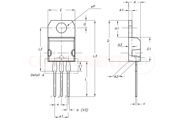
| Dimension Symbol | Minimum (mm) | Typical (mm) | Maximum (mm) | Mechanical Description |
| A | 4.40 | 4.45 | 4.50 | Main plastic body thickness/depth |
| A1 | 1.22 | - | 1.32 | Metal mounting tab thickness |
| A2 | 2.49 | 2.59 | 2.69 | Distance from tab to lead seating plane |
| A3 | 1.17 | 1.27 | 1.37 | Step thickness to mounting tab |
| b | 0.78 | - | 0.87 | Lead width (all 3 terminals) |
| b2 | 1.25 | - | 1.34 | Upper lead width section (Pins 1 & 3) |
| b4 | 1.20 | - | 1.29 | Upper lead width section (Pin 2) |
| c | 0.49 | - | 0.56 | Lead thickness |
| D | 15.40 | 15.50 | 15.60 | Total package body height |
| D1 | 9.05 | 9.15 | 9.25 | Plastic mold case body height |
| E | 10.08 | 10.18 | 10.28 | Package body width |
| e | 2.44 | 2.54 | 2.64 | Lead pitch spacing between adjacent pins |
| e1 | 4.98 | 5.08 | 10.185.18 | Total lead pitch spacing (Pin 1 to Pin 3) |
| H1 | 6.25 | 6.35 | 6.45 | Height of mounting tab above plastic body |
| L | 13.20 | 13.40 | 13.60 | Lead length below seating plane |
| L1 | 3.50 | 3.70 | 3.90 | Transition lead length below mold body |
| ∅P | 3.75 | 3.80 | 3.85 | Mounting hole diameter |
| Q | 2.70 | 2.80 | 2.90 | Hole center distance to top of package |