2N6107 PNP Power Transistor
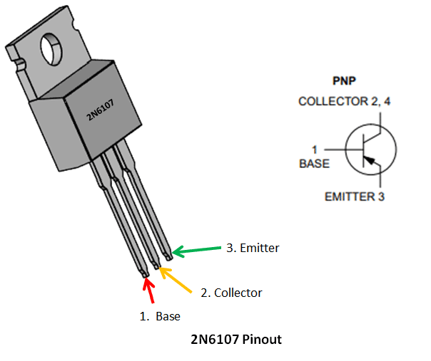
2N6107 Pin Configuration
|
Pin No. |
Pin Name |
Description |
|
1 |
Base |
Controls the biasing of transistor, Used to turn ON or OFF the transistor |
|
2 |
Collector |
Current flows in through collector, normally connected to load |
|
3 |
Emitter |
Current Drains out through emitter, normally connected to ground |
Features and Specifications
- TO−220 Compact Package
- 2N6017 is a PNP power transistor
- VCBO Collector Base Voltage 80 Vdc
- VCEO Collector Emitter Voltage 70 Vdc
- VEB Emitter−Base Voltage 5V Vdc
- Maximum Base Current IB 3.0 A
- Collector Current − Continuous IC 7.0 A
- Collector Current − Peak ICM 10 A
- Total Power Dissipation PD - 40 W
- High DC Current Gain
- High Current Gain − Bandwidth Product
Equivalent
NTE197 (PNP), 2N6110 (PNP).
Brief about 2N6107 Transistor
2N6107 is a PNP transistor and has a gain value of 30 to 150; this value determines the amplification capacity of the transistor. The maximum amount of current that could flow through the Collector pin is 7A, hence we cannot connect loads that consume more than 7A using this transistor. To bias a transistor we have to supply current to base pin, this current (IB) should be limited to 3A and voltage across the base emitter pin should be 5V.
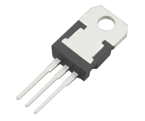
When this transistor is fully biased then it can allow a maximum of 7A to flow across the collector and emitter. Base-Emitter ON Voltage VBE (ON) under the condition that collector current IC is 7A and Collector-Emitter voltage VCE is 4 Vdc is 3 Vdc maximum. 2N6107 comes with TO−220 Compact Packaging, which has a metal tab which acts as an electrical collector pin and also acts as heat dissipation for the high power range of the transistor.
2N6017 can be used as power amplifiers and switching applications.
How to use a PNP Transistor?
The main working principle of a PNP transistor is, when the current exists at the base of the PNP transistor, and then the transistor remains OFF. When there is no flow of current at the base of the transistor, the transistor switches ON.
The current is sinked into the PNP transistor and current flows from emitter to collector and this is the main difference between the NPN and PNP transistor. To switch ON a PNP transistor, you need the base voltage to be less than the emitter voltage. This is because the base terminal is made-up of a n-type semiconductor and emitter is made-up of p-type semiconductor.
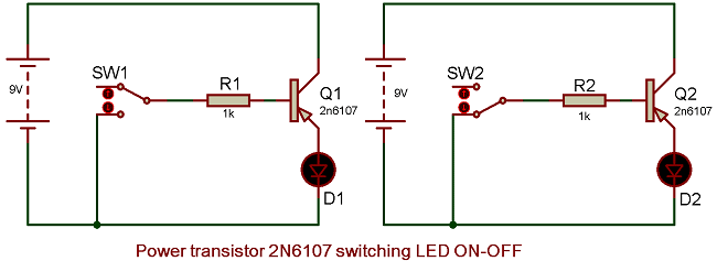
Therefore in above circuit the emitter voltage is kept higher than base voltage by connecting power source’s (9V DC battery) positive terminal to the emitter and its negative terminal to the base.
Diode is connected towards the emitter side or ground terminal of the transistor. It will get turn ON when the base voltage is less than emitter voltage or is 0V and remains OFF when the base voltage is higher than the emitter voltage.
High load can be replaced by the LED and 2N6107 can be used to run high current loads efficiently due to its high power capacity.
Applications
- Driver Modules like Relay Driver, LED driver etc.
- Amplifier modules like Audio amplifiers, signal Amplifier etc.
- Darlington pair
2D-Model (PDIP)