2N2646 Unijunction Transistor
2N2646 is general purpose silicon PN Unijunction Transistor that is designed for general purpose industrial applications. The device is popular as a triggering device and is not suited for driving power loads.
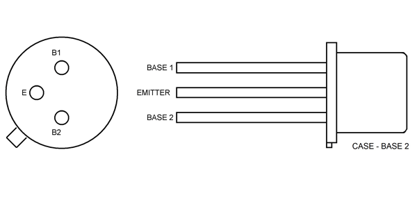
Pin Configuration
2N2646 is a three terminal device and the conductive case also connected to a terminal.
|
Pin |
Name |
Description |
|
1 |
Base 1 |
Normally connected to Power |
|
2 |
Emitter |
Emitter is used for triggering transistor ON and OFF |
|
3 |
Base 2 |
Normally connected to Load |
|
|
Case |
Connected to Base 2 pin internally |
2N2646 Features and Specifications
- Available as “HR” (high reliability)
- Available as non-RoHS (Sn/Pb plating)
- Low emitter reverse current: 0.005µA (Typ)
- PASSIVATED surface for reliability and uniformity
- Maximum voltage between two bases (VB2B1): 35V
- Maximum emitter reverse voltage (VB2E): 30V
- Maximum RMS emitter current (Ie): 50mA
- Maximum peak emitter current (Ie): 2A
- Operating temperature range: -65ºC to +150ºC
- Maximum power dissipation : 300mW
Similar Transistors
2N2647, 2N4870, 2N4871, 2N1671
2N2646 Overview
2N2646 is mainly used for designing firing circuits (for Silicon Controlled Rectifiers) and not used for amplifier circuits like transistors. The device is preferred in other applications where guaranteed minimum pulse amplitude is required and also where a low emitter leakage current and a low peak point emitter current (trigger current) are required. 2N2646 applications can be found in many low cost industrial applications.
How to use 2N2646 Transistor
2N2646 has many application circuits but for understanding the working let us consider the relaxation oscillator circuit of the device.
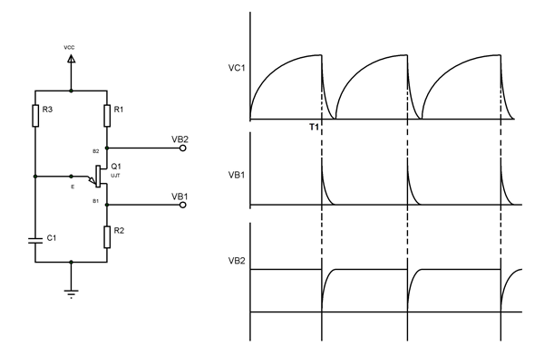
In the above circuit we are working 2N2646 as a relaxation oscillator to produce trigger pulses or oscillations. The resistors R1 and R2 are for limiting the current going through UJT. The capacitor C1 is for triggering the UJT and resistor R3 is for limiting the flow of charge to capacitor. The circuit is powered from single power source of VCC.
Working
When the power just turned ON, the UJT will be in high resistance state and total supply voltage appears across it. So under initial state VB2 (or UJT voltage drop) will be equal VCC as shown in the graph. With the flow of time the capacitor gets charged as the current flows through R3 to reach the capacitor. Once the capacitor gets charged to threshold voltage at a certain time T1, it will discharge by forcing the current through emitter of the UJT. With this current flow at the emitter the UJT will get from high resistance to low resistance state and there by acting as a short circuit. Under such case we will have VB2 (or UJT voltage drop) taking a sharp dip as shown in graph and at other hand because of current flow a voltage appears across R2 (VB1) there by producing a sharp pulse voltage as shown in graph.
With completion of capacitor discharge the UJT will again return to normal OFF state and will stay in that state until the capacitor discharges again. This cycle of capacitor charge and discharge form a triggering cycle for the UJT to give voltage pulses at the output or VB2. By this we have UJT acting as an oscillator giving voltage pulses at the output and in a similar way we can use the device in other application circuits.
Applications
- General purpose industrial applications
- SCR firing circuits
- Hobby projects
- Phase control circuit
- Saw tooth wave generator
- Timing circuit
- Voltage detector
- Relaxation oscillator
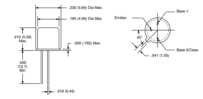
2D-Model
Measurements in inches and measurements in millimeter are in bracket