BT169 Sensitive Gate SCR Pinout, Variants, Equivalent & Datasheet
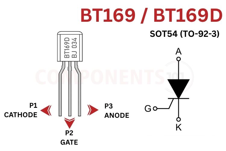
BT169 Pinout Configuration
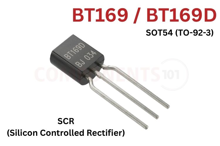
The BT169 is housed in the plastic single-ended TO-92 (SOT54) package. When viewing the flat front face of the device, the terminal arrangement from left to right is summarised below:
| Pin Number | Pin Name | Terminal Type | Functional Description |
| 1 | Cathode (K) | Common Return | Negative reference terminal connected to circuit ground or AC neutral. |
| 2 | Gate (G) | Control Terminal | Sensitive control terminal. Positive current injection initiates latching. |
| 3 | Anode (A) | Main Power Terminal | Positive power conduction terminal connected in series with the load. |
*Note: In the standard TO-92 (SOT54) casing, the middle pin is the Gate terminal, unlike standard bipolar junction transistors where the middle lead is typically the Collector or Base.
BT169 Voltage Variants & Marking Codes
The BT169 series is available in multiple repetitive peak off-state voltage grades indicated by the letter suffix. The BT169 is a 0.8 A (RMS) sensitive-gate thyristor (SCR) in a TO-92 package. The most common commercial and industrial variant is the 400V-rated BT169D:
| Part Number | Voltage Rating (VDRM / VRRM) | Package Type | Marking Code | Primary Applications |
| BT169B | 200V | TO-92 (SOT54) | BT169B / BT169BH | 24V/48V DC telecom circuits, automotive electronics, and low-voltage relays. |
| BT169D | 400V | TO-92 (SOT54) | BT169D / BT169DH | Standard 120V AC line switching, 230V rectified DC rails, and power supplies. |
| BT169E | 500V | TO-92 (SOT54) | BT169E / BT169EH | 230V AC consumer electronics, capacitive ignition, and sensor latching. |
| BT169G | 600V | TO-92 (SOT54) | BT169G / BT169GH | High-voltage 230V/240V AC industrial mains with high transient voltage headroom. |
*Note: The suffix 'H' in the marking code (e.g. BT169DH) indicates high-temperature factory manufacturing and halogen-free assembly molding compound.
BT169 Key Features & Specifications
- Device Type: Sensitive Gate Silicon Controlled Rectifier (SCR / Thyristor)
- Repetitive Peak Off-State Voltage (VDRM): 400V (BT169D) / 500V (BT169E) / 600V (BT169G)
- Repetitive Peak Reverse Voltage (VRRM): 400V (BT169D) / 500V (BT169E) / 600V (BT169G)
- RMS On-State Current (IT(RMS)): 0.8 A (half-sine wave, Tlead ≤ 83°C)
- Average On-State Current (IT(AV)): 0.5 A (half-sine wave, Tlead ≤ 83°C)
- Non-Repetitive Peak Surge Current (ITSM): 8.0 A (tp = 10 ms half-sine) / 9.0 A (tp = 8.3 ms)
- Peak Gate Current (IGM): 1.0 A
- Peak Reverse Gate Voltage (VRGM): 5.0 V
- Gate Trigger Current (IGT): 50 µA typ, 200 µA max (at VD = 12V, IT = 10 mA, Tj = 25°C)
- Gate Trigger Voltage (VGT): 0.5V typ, 0.8V max (at VD = 12V, IT = 10 mA, Tj = 25°C)
- Latching Current (IL): 2.0 mA typ, 6.0 mA max (at VD = 12V, IG = 0.5 mA, Tj = 25°C)
- Holding Current (IH): 2.0 mA typ, 5.0 mA max (at VD = 12V, Tj = 25°C)
- On-State Forward Voltage Drop (VT): 1.25V typ, 1.7V max (at IT = 1.2 A, Tj = 25°C)
- Gate Turn-On Time (tgt): 2.0 µs typ (at ITM = 2 A, VD = 400V, IG = 10 mA)
- Operating Junction Temperature Range (Tj): -40°C to +125°C
- Storage Temperature Range (Tstg): -40°C to +150°C
*Note: Complete Technical Details can be found in the BT169 datasheet given at the end of this page.
BT169 Equivalent & Alternative Components
Which BT169 equivalent should you choose? Match the package, pinout, voltage, current and gate sensitivity. Parts in the first table are close substitutes, but you should still check the pinout in the substitute's datasheet.
| Equivalent Part | Package | Max VDRM | Max IT(RMS) | Gate Sensitivity (IGT) | Key Features & Applications |
| 2N5064 | TO-92 | 200V | 0.8 A | ≤ 200 µA | Classic JEDEC-sensitive gate SCR; lower voltage rating than BT169D. |
| MCR100-6 | TO-92 / SOT-89 | 400V | 0.8 A | ≤ 200 µA | Widely deployed direct drop-in replacement; identical pinout and ratings. |
| PCR406 | TO-92 | 400V | 0.8 A | ≤ 200 µA | Common consumer electronics equivalent; directly pin-compatible. |
| C106D | TO-126 | 400V | 4.0 A | ≤ 200 µA | Sensitive gate SCR with higher continuous current (4A) in a tabbed package. |
| EC103D | TO-92 | 400V | 0.8 A | ≤ 200 µA | Littelfuse sensitive SCR equivalent for appliance and ballast switching. |
| BT151-500R | TO-220AB | 500V | 12 A | ≤ 15 mA | High-power industrial-standard SCR requires higher gate drive current. |
| BT149 | TO-92 | 100V - 600V | 0.8 A | ≤ 200 µA | Sibling series from WeEn/NXP; functionally identical to BT169. |
What Is the BT169 Thyristor?
The BT169 is a four-layer PNPN regenerative semiconductor switch. Unlike bipolar transistors that require sustained base current to maintain conduction, or MOSFETs that rely on electrostatic gate charge, an SCR functions as a bistable solid-state latch. When forward-biased (Anode positive relative to Cathode), the central reverse-biased PN junction blocks current flow, maintaining the device in a high-impedance forward-blocking state with leakage current below 0.1 mA.
When a small positive current pulse (exceeding IGT = 200 µA) is injected into the Gate-Cathode junction, the internal NPN and PNP transistor sections enter positive feedback. The NPN transistor drives the base of the PNP transistor, and the PNP collector in turn feeds the base of the NPN transistor. This regenerative cascade drives both internal transistor sections into deep saturation within 2 µs, collapsing the anode-to-cathode voltage drop to a low forward conduction level (VT ≈ 1.25V).
Once triggered, the Gate terminal completely loses control over conduction. The BT169 will remain latched in the ON state indefinitely, even if the gate current is completely removed. Conduction can only be extinguished by reducing the anode current below the holding current threshold (IH = 2 mA to 5 mA) through external means, such as interrupting the DC supply rail, commutating the voltage across zero (natural AC zero-crossing), or momentarily shunting the anode to cathode.
Because of its sensitive gate construction, the BT169 can be vulnerable to false triggering caused by rapid voltage transients across the anode and cathode (dv/dt effect) or capacitive displacement currents. Connecting an external gate-to-cathode pull-down resistor (RGK = 1 kΩ) shunts internal junction displacement currents safely to ground, elevating the critical rate of voltage rise (dVD/dt) from 25 V/µs up to 800 V/µs, ensuring rock-solid noise immunity in electrically noisy environments.
BT169 Datasheet
Download the official manufacturer BT169 datasheet for the BT169 Sensitive Gate Silicon Controlled Rectifier:
BT169 Circuit Diagram: DC Latching Switch and Relay Driver
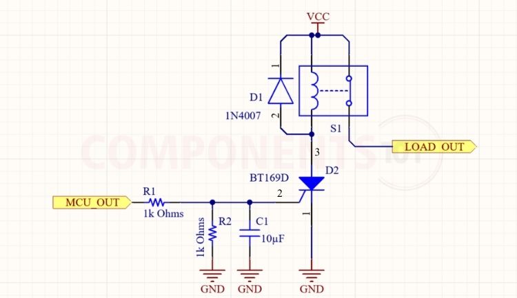
The BT169 is commonly deployed in DC Latching Switch circuits, overvoltage crowbar protection stages, and microcontroller-driven relay actuators. The schematic below illustrates a robust, pop-free DC Latching Switch and Relay Driver designed to interface directly with 3.3V or 5V logic controllers.
Circuit Operation & Component Selection
The circuit uses a 12V DC supply to control a 12V relay through a BT169 SCR, with a 1N4007 flyback diode protecting against inductive voltage spikes. A 1 kΩ gate resistor limits trigger current, while a 1 kΩ gate-to-cathode resistor and 10 nF capacitor improve noise immunity. When a 3.3V or 5V trigger pulse is applied, the SCR turns ON and latches, keeping the relay energized even after the trigger is removed. The relay remains active until the normally closed RESET pushbutton interrupts the supply current, allowing the SCR to turn OFF and return to standby.
BT169 Applications
- DC Latching Switches & Relay Controllers: Low-power solid-state memory switches that maintain energized states without continuous microcontroller gate power.
- Overvoltage Crowbar Protection: High-speed protection clamp in 5V/12V linear and switch-mode power supplies; triggers instantly when a Zener voltage is exceeded to blow a protective fuse.
- Capacitive Discharge Ignition (CDI): Discharge switch in small engine ignitions, chainsaws, lawn mowers, scooters, and motorcycle electronic ignition modules.
- Ground Fault Circuit Interrupters (GFCI): High-reliability trip actuator in residual current circuit breakers and leakage current protection outlets.
- Strobe Lights & Camera Flash Triggers: Discharging high-voltage trigger capacitors through pulse transformers to ionize xenon flashtubes.
- Electronic Ballasts & Gas Igniters: Pulse firing in fluorescent lighting starters, gas oven igniters, and arc furnace controllers.
- Security & Alarm Systems: Latching detector circuits that remain triggered upon sensor trip until manually reset by an operator.
BT169 2D Model and Component Dimensions
For engineers creating custom footprints in CAD software (KiCad, Altium Designer, Eagle, EasyEDA), the mechanical dimensions for the standard TO-92 (SOT54) plastic through-hole package from the official NXP / WeEn datasheet are detailed below:
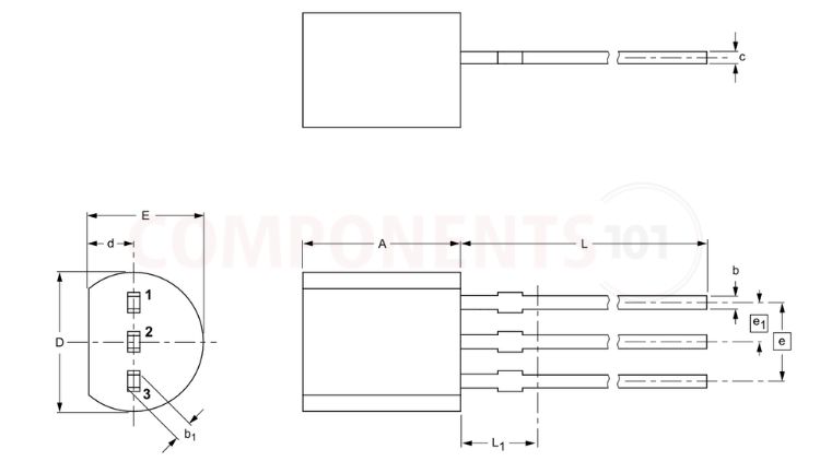
| Dimension Parameter | Symbol | Min (mm) | Typ (mm) | Max (mm) | Min (Inches) | Max (Inches) |
| Package Body Height | A | 5.0 | 5.1 | 5.2 | 0.197 | 0.205 |
| Lead Width / Diameter | b | 0.40 | 0.44 | 0.48 | 0.016 | 0.019 |
| Lead Thickness | c | 0.38 | 0.41 | 0.45 | 0.015 | 0.018 |
| Package Body Width | D | 4.4 | 4.6 | 4.8 | .0.173 | 0.189 |
| Body Depth from Flat | d | 1.4 | 1.55 | 1.7 | 0.055 | 0.067 |
| Total Body Depth / Thickness | E | 3.6 | 3.9 | 4.2 | 0.142 | 0.165 |
| Lead Length | L |
12.7 |
13.6 | 14.5 | 0.500 | 0.571 |
| Outer Lead Pitch (Pin 1 to Pin 3) | e | - | 2.54 | - | - | 0.100 |
| Adjacent Lead Pitch (Pin 1 to Pin 2) | e1 | - | 1.27 | - | - | 0.050 |