2N1595 - Silicon Thyristor
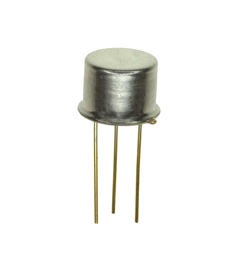
2N1595 is a solid state semiconductor device called Thyristor or SCR (Silicon Controlled Rectifier). It is an industrial-type, low-current device available in a three-lead package ideal for printed-circuit applications.
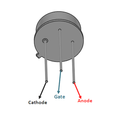
Pin configuration
2N1595 is a three pin device as shown in above diagram and we will describe each of these pins below.
|
Pin |
Name |
Function |
|
1 |
Cathode |
Connected to neutral |
|
2 |
Gate |
Low voltage trigger pulse is given to this pin |
|
3 |
Anode |
Connected to Load |
Features and Electrical characteristics of 2N1595
- High reliability
- Available as non-RoHS (Sn/Pb plating)
- Body case suitable for fixing heat sink
- Peak reverse blocking voltage: 50V
- Peak surge current: 15A
- Peak gate current: 0.1A
- Peak gate voltage: 10V
- Peak repetitive current handling capability of 1.6 amperes @125°C
- Operating junction temperature range: -65ºC to +125ºC
- Storage Temperature Range: -65ºC to +150ºC
- Turn-On Time: 0.8µS
- Turn-Off Time: 10µS
Similar Thyristors
2N1596, 2N1597, 2N1598, 2N1599
Overview of 2N1595 SCR
2N1595 is a device basically used in low voltage AC rectifying applications and unlike diode DC converter the rectifier designed by this device will be of controlled one. Multiple devices can be used to form fully controller AC rectifier where RMS output voltage can be controller through controlled triggering of the device.
2N1595 is used in many AC rectifier and RMS voltage controller applications.
How to use 2N1595 SCR
First let us consider a simple application circuit for the device as shown in the circuit diagram below. Here V1 is the AC voltage source, Load is a 20Ω resistor and Vg is the trigger pulse given to the gate of the device. Also in circuit, device Anode is connected to load and cathode is connected to second end of power source.
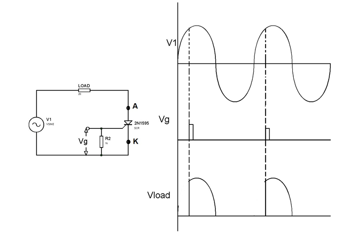
Now at any given time the sinusoidal wave for the source can be draw as shown in first graph of the above picture. Under no trigger to the gate of the SCR (i.e. Vg =0V), the total drop appears across the device and we have Vload = 0V. This state continuous until a pulse is give to the gate of the device and with that the SCR starts conducting until the half cycle completes and V1 reaches the zero. During the period of SCR conduction a voltage appears across the load due to current flow and is shown in the graph.
For the negative cycle the SCR will be reverse biased and there will be no current flow in the circuit even in the presence of the trigger.
With the following half cycle another trigger is needed for the SCR to get from high resistance state to low resistance state and also we can change the trigger timing as per requirement. As given in graph the voltage across the load follows the V1 source after the trigger is given.
Applications
- AC rectifiers
- RMS voltage switching
- Power regulators
- SMPS (Switch Mode Power Supply)
- Power converters
- Industrial switching
2D-Model