J111 N-Channel JFET Transistor Pinout, Marking Code, Equivalent & Datasheet
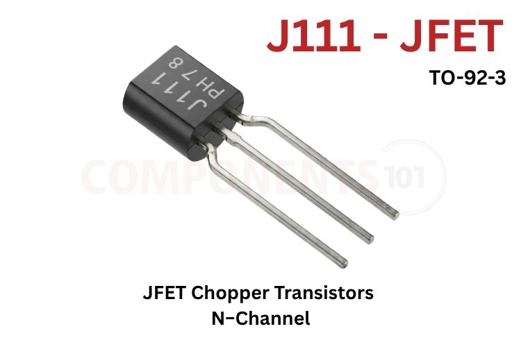
The J111 JFET is an N-channel junction FET built for low-level analog switching, sample-and-hold circuits and chopper-stabilised amplifiers. Below you will find the J111 pinout, J111 datasheet specifications, J111 equivalents, and a J111 circuit diagram for pop-free audio muting.
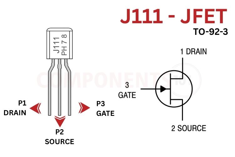
The standard J111 is housed in the standard TO-92 package. The terminal designations are summarised below:
| Pin Number | Pin Name | Terminal Type | Functional Description |
| 1 | Drain (D) | Channel Terminal | Drain terminal for analog current flow. Electrically interchangeable with Source. |
| 2 | Source (S) | Channel Terminal | Source terminal for analogue current flow. Electrically interchangeable with Drain. |
| 3 | Gate (G) | Control Terminal | P-type gate junction controlling the depletion region and channel conduction. |
*Note: Due to the symmetrical planar design of junction field-effect transistors, Pins 1 and 2 (Drain and Source) can be interchanged in analog switching and muting circuits without degrading performance.
J111 Package & SMD Marking Codes
The J111 is manufactured in both leaded through-hole and surface-mount packaging formats. For space-constrained SMT printed circuit boards, the device is marketed under the MMBFJ111 designation in the miniature SOT-23 package:
| Part Number | Package Type | Marking Code | Mounting Style | Key Features & Notes |
| J111 / J111G | TO-92 (Case 29-11) | J111 | Through-Hole | Industry standard 3-pin package; Pb-free version denoted by 'G' suffix. |
| MMBFJ111 | SOT-23 (TO-236) | 6X / M6X | Surface Mount | Sub-miniature SMD footprint; identical electrical ratings to TO-92 J111. |
| J111RL1G | TO-92 (Tape & Reel) | J111 | Automated Insertion | Radial lead tape-and-reel packaging for high-volume automated PCB pick-and-place. |
*Note: SOT-23 top markings may include date codes, manufacturer location identifiers, or orientation dots adjacent to the 6X primary alphanumeric code.
J111 Key Features & Specifications
- Transistor Polarity & Type: N-Channel Depletion-Mode Junction FET (JFET)
- Drain-Gate Voltage (VDG): 35V
- Gate-Source Voltage (VGS): -35V
- Gate-Source Breakdown Voltage (V(BR)GSS): 35V min (at IG = -1.0 µA)
- Zero-Gate-Voltage Drain Current (IDSS): 20 mA min (at VDS = 15V, VGS = 0V)
- Gate-Source Cutoff Voltage (VGS(off)): -3.0V to -10V (at VDS = 5.0V, ID = 1.0 µA)
- Static Drain-Source On-Resistance (rDS(on)): 30 Ω max (typ. 15 Ω - 20 Ω at VDS = 0.1V, VGS = 0V)
- Gate Reverse Current (IGSS): 1.0 nA max (at VGS = -15V, VDS = 0V)
- Drain-Cutoff Current (ID(off)): 1.0 nA max (at VDS = 5.0V, VGS = -10V)
- Input / Inter-Electrode Capacitance (Cdg(on) + Csg(on)): 28 pF max (at VDS = VGS = 0V, f = 1.0 MHz)
- Turn-On Delay / Rise Time (td(on) / tr): 4.0 ns typ / 6.0 ns typ (at ID = 20 mA)
- Turn-Off Delay / Fall Time (td(off) / tf): 6.0 ns typ / 25 ns typ (at ID = 20 mA)
- Maximum Power Dissipation (PD): 350 mW (TO-92 at TA = 25°C, derating 2.8 mW/°C)
- Operating Junction & Storage Temperature: -65°C to +150°C
- Lead Solder Temperature (TL): 300°C (maximum 10 seconds duration)
*Note: Complete Technical Details can be found in the J111 datasheet given at the end of this page.
J111 Equivalent & Alternative Components
The right J111 equivalent depends on what you need to keep: the package, the low on-resistance, or the gate-drive voltage. Check VGS(off) and rDS(on) first, because a substitute with a shallower cutoff or higher resistance changes muting depth and distortion.
| Equivalent Part | Polarity | Max VDS | Max rDS(on) | Min IDSS | Cutoff VGS(off) | Package & Description |
| MMBFJ111 | N-Channel | 35V | 30 Ω | 20 mA | -3.0V to -10V | SOT-23 surface-mount, identical die equivalent. |
| J112 | N-Channel | 35V | 50 Ω | 5.0 mA | -1.0V to -5.0V | Higher on-resistance; lower gate cutoff voltage requirement. |
| J113 | N-Channel | 35V | 100 Ω | 2.0 mA | -0.5V to -3.0V | Sensitive gate cutoff (-0.5V to -3V); suited for lower logic levels. |
| 2N5432 | N-Channel | 25V | 5.0 Ω | 100 mA | -4.0V to -10V | Ultra-low on-resistance analog switch; higher-power TO-52 can. |
| 2N4391 | N-Channel | 40V | 30 Ω | 50 mA | -4.0V to -10V | High-voltage military/industrial JFET chopper in metal TO-18 can. |
| MPF102 | N-Channel | 25V | 200 Ω | 2.0 mA | -0.5V to -8.0V | General-purpose RF/VHF amplifier JFET in TO-92 package. |
| J201 | N-Channel | 40V | 1.5 kΩ | 0.2 mA | 0.3V to -1.5 V | High-gain audio preamp JFET; not suited for low-impedance switching. |
Brief Description of J111
The J111 belongs to the renowned J111/J112/J113 family of silicon N-channel junction field-effect transistors specifically tailored for low-resistance switching. Unlike enhancement-mode MOSFETs that require a positive gate-to-source bias to induce an inversion layer, the J111 features a naturally doped N-type conduction channel spanning from drain to source. In the absence of an applied gate bias (VGS = 0V), majority carrier electrons flow unobstructed between drain and source, presenting an exceptionally low channel resistance of rDS(on) ≤ 30 Ω.
A key operational advantage of JFETs over bipolar junction transistors (BJTs) in analog switching is the complete absence of a collector-emitter saturation voltage offset (VCE(sat) = 0V). This enables true bilateral, microvolt-level signal transmission with near-zero harmonic distortion. Furthermore, unlike MOSFETs that incorporate an intrinsic body-drain PN junction diode, the JFET has no parasitic substrate diode shunting the channel. This prevents unintended signal clipping or reverse conduction when handling bipolar AC signals, provided the gate junction remains reverse-biased relative to both source and drain.
To switch the J111 OFF, the gate terminal must be driven significantly negative with respect to the source and drain terminals. When VGS reaches the cutoff voltage VGS(off) (specified between -3.0 V and -10V for the J111), the reverse-biased PN junction depletion regions expand and merge across the entire channel cross-section, terminating carrier flow. Because the J111 requires up to -10V for full cutoff, circuit designs operating on bipolar supplies (such as ±12V or ±15V) provide the ideal control voltage headroom.
J111 Datasheet
Download the official manufacturer J111 datasheet for the J111 N-Channel JFET Chopper Transistor. The same document covers the J111, J112, J113 and the SOT-23 MMBFJ111, MMBFJ112 and MMBFJ113, including ratings, electrical characteristics, thermal data, package drawings and marking diagrams.
J111 Circuit Diagram: Pop-Free Audio Muting
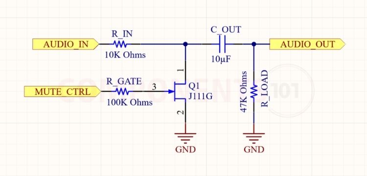
The J111 is frequently deployed as a shunt analog switch or pop-free audio muting circuit in audio DACs, preamplifiers, and mixing consoles. In the J111 circuit diagram below configuration, the J111 shunts unwanted transient clicks, power-down pops, or muted signals directly to analog ground.
How to Use the J111 in a Circuit Operation & Component Selection
The J111 JFET provides audio muting through shunt switching. The input audio signal passes through a 10 µF coupling capacitor and a 10 kΩ series resistor, while the J111 connects the signal path to analog ground. When the MUTE control is at -12V, the JFET turns OFF, allowing the audio signal to pass with minimal attenuation. When the control is at 0V, the JFET turns ON, shunting the signal to ground and providing approximately 50 dB of attenuation. A 2N3904 or BC547 NPN transistor can interface the circuit with 3.3V or 5V microcontroller GPIOs, enabling software-controlled muting during power transitions or track changes without mechanical relay noise.
Applications
- Pop-Free Audio Muting: Suppressing power-up thumps and switching pops in DAC outputs, home theatre amplifiers, and studio mixing consoles.
- Precision Analog Commutators: High-speed bilateral signal multiplexing and signal routing in data acquisition systems.
- Sample-and-Hold Circuits: Low-leakage sampling switches in analog-to-digital converters and precision measurement instrumentation.
- Voltage-Controlled Attenuators (VCR): Operating in the ohmic/triode region as an electrically tunable analog resistor for automatic gain control (AGC).
- Chopper-Stabilized Amplifiers: Low-frequency AC modulation of microvolt DC instrumentation signals to eliminate op-amp 1/f flicker noise and DC drift.
- RF & Video Signal Gating: Fast RF signal gating and baseband switching with minimal inter-terminal parasitic capacitance.
- Solid-State Relays: Fast, bounce-free replacement for mechanical reed relays in low-level signal testing equipment.
2D Model and Component Dimensions
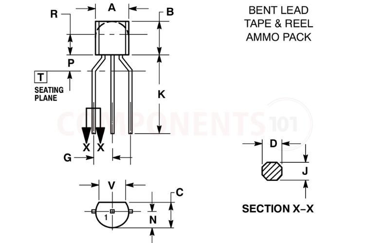
For PCB layout engineers and CAD designers creating footprints in KiCad, Altium Designer, Eagle, or EasyEDA, the mechanical dimensions for the standard through-hole TO-92 (Case 29-11, Style 5) package are listed below:
| Dimension Parameter | Symbol | Min (mm) | Typ (mm) | Max (mm) | Min (Inches) | Min (Inches) |
| Package Body Height | A | 4.45 | 4.82 | 5.20 | 0.175 | 0.205 |
| Package Body Width | B | 4.32 | 4.80 | 5.33 | 0.170 | 0.210 |
| Package Body Depth / Thickness | C | 3.18 | 3.68 | 4.19 | 0.125 | 0.165 |
| Lead Width / Diameter | D | 0.407 | 0.457 | 0.533 | 0.016 | 0.021 |
| Lead Pitch (Pin 1 to Pin 2) | G | 1.15 | 1.27 | 1.39 | 0.045 | 0.055 |
| Lead Spacing (Pin 1 to Pin 3) | H | 2.42 | 2.54 | 2.66 | 0.095 | 0.105 |
| Lead Thickness | J | 0.39 | 0.45 | 0.50 | 0.015 | 0.020 |
| Lead Length | K | 12.70 | - | - | 0.500 | - |
| Lead Seating Width | N | 2.04 | 2.35 | 2.66 | 0.080 | 0.105 |