74LS04 - Hex Inverting Gates
- 74LS04 is a member of 74XXYY IC series. The 74-series are digital logic integrated circuits.
- 74LS04 IC has six NOT gates. These NOT gates perform Inverting function. Hence name HEX INVERTING GATES.
74LS04 Pin Configuration
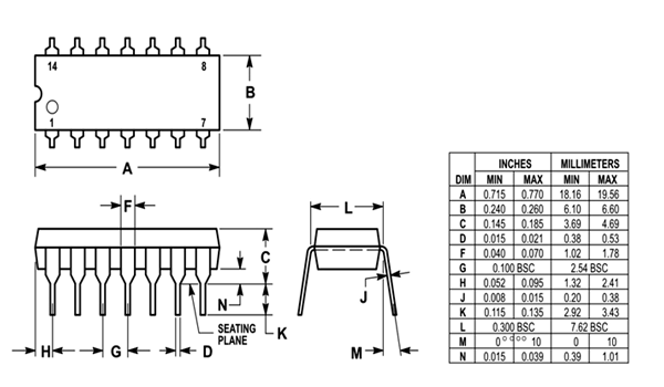
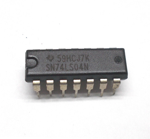
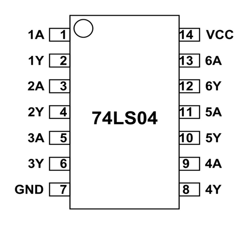
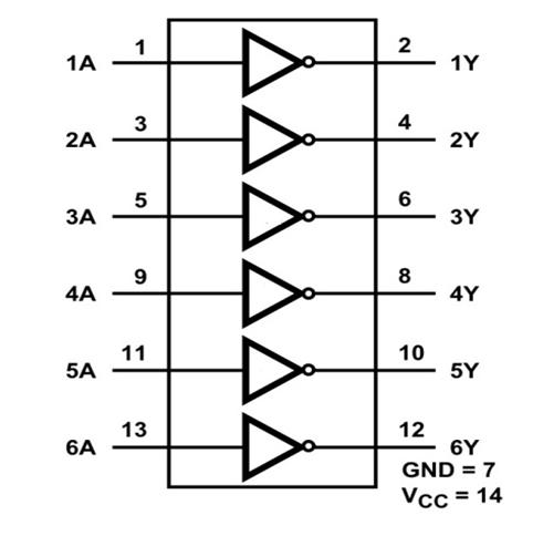
74LS04 is a14 PIN IC as shown in the 74LS04 pinout. This IC is available in various packages. Choose the appropriate package depending on requirement. The description for each pin is given below.
|
Pin Number |
Description |
|
INPUT OF INVERTING GATES |
|
|
1 |
1A-INPUT of GATE 1 |
|
3 |
2A-INPUT of GATE 2 |
|
5 |
3A-INPUT of GATE 3 |
|
9 |
4A-INPUT of GATE 4 |
|
11 |
5A-INPUT of GATE 5 |
|
13 |
6A-INPUT of GATE 6 |
|
SHARED TERMINALS |
|
|
7 |
GND- Should be connected to ground |
|
14 |
VCC-Should be connected to positive voltage |
|
OUTPUT OF INVERTING GATES |
|
|
2 |
1Y-OUTPUT of GATE 1 |
|
4 |
2Y-OUTPUT of GATE 2 |
|
6 |
3Y-OUTPUT of GATE 3 |
|
8 |
4Y-OUTPUT of GATE 4 |
|
10 |
5Y-OUTPUT of GATE 5 |
|
12 |
6Y-OUTPUT of GATE 6 |
74LS04 Features and Specifications
- Supply voltage range: +4.75V to +5.25V
- Maximum supply voltage: +7V
- Maximum current allowed to draw through each gate output: 8mA
- Totally lead free
- TTL outputs
- MaximumRise Time: 15ns
- Maximum Fall Time: 15ns
- Operating temperature:0°C to 70 °C
Note: Complete technical information can be found in the 74LS04 Datasheet linked at the bottom of this page.
74LS04 Equivalents
CD7404, 74LS14, A single transistor can be configured to form a NOT gate.
Where to Use 74LS04 IC?
Here are few cases where 74LS04 is used.
1. The chip is basically used where a logic inverter is needed. Inverter Gates in this chip provide output which is negated logic input. The chip has six gates which do NOT operation.
2. When you want TTL outputs. The gates in this chip provide TTL logic outputs which are a must in some applications.
3. 74LS04 is a low cost chip available in market and so it is used when application cost is low.
How to use 74LS04
As mentioned earlier 74LS04 has six INVERTING GATES which can be used individually. The internal connection of gates can be given as below.
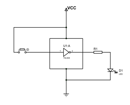
Now let us take a single gate of the six and connect it as shown in circuit diagram.
For understanding the working of NOT gate, let’s redraw it in more simplified version.
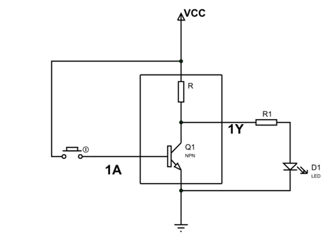
As shown in diagram, we have a transistor forming a NOT gate. Input here is 1A which is connected to button. Output 1Y is connected to LED through a resistor. The LED is connected to know the output status.
In the circuit,
When button is not pressed:
Current through base of transistor will be zero. Because base current is zero the transistor will be in OFF state. Under OFF sate the total supply voltage appears across the transistor.Under such case the output 1Y here will be HIGH, since output is nothing but voltage across transistor. Hence when button is not pressed INPUT 1A = LOW and OUTPUT 1Y = HIGH.
When button is pressed:
Voltage appears at base of transistor and current flows through it. Because base current is present the transistor will turn ON. Under ON sate the total supply voltage appears across the resistor and voltage across transistor will be zero. Under such case the output 1Y here will also be LOW, since output is nothing but voltage across transistor. Hence when button is pressed INPUT 1A = HIGH and OUTPUT 1Y = LOW.
If we draw truth table based on above cases, we will have.
|
Input 1A |
Output 1Y |
|
LOW |
HIGH |
|
HIGH |
LOW |
By truth table you can understand that OUTPUT for NOT gate is negation or inversion of INPUT. We can write the output function as, Y = A .
We have six of these gates in 74LS04 chip. We can use one or all six of these gates depending on requirement.
Applications
- General purpose logic
- Servers
- Memory units
- PCs and notebooks
- Digital Electronics
- Networking
- Digital systems
2D Model
