FemtoClock2: Family of Small and Low Power 75fs Jitter Clocks for Cost-Effective and Simple Clock Tree Implementation
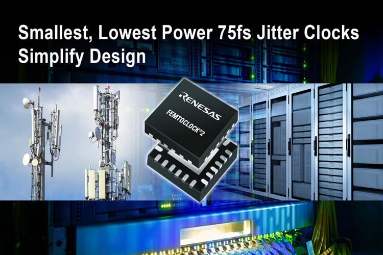
Renesas Electronics Corporation has expanded its timing solution portfolio with the new sub-100fs point-of-use clock solution for data center, server, and network infrastructure markets. The new FemtoClock2 family was designed to provide cost-effective and simple clock tree implementation for next-generation, high-speed interconnect designs by offering ultra-low jitter clock generators and jitter attenuators in a small 4x4mm2 package.
The 64fs RMS low jitter of the FemtoClock2 allows the customers to easily meet next-generation PAM4 requirements on new switch or router designs. The small 4x4mm2 form factor of the FemtoClock2 family allows the designers to place the clock source at the point of use for streamlined PCB layout design reduced cross talk and cleaner signals. FemtoClock2 can be configured as a DCO, clock generator, or jitter attenuator, offering valuable design flexibility and reuse.
Features of FemtoClock2 Family
- As low as 64fs (typ) RMS jitter
- Low power consumption of 600mW
- 4x4 mm2 in 24- and 28-pin QFN packages
- Single & dual input options with four differential outputs
- Power supply noise rejection better than -80dB
- Output-to-output isolation of -80dBc
- Compliant with ITU-T G.8262 and G.8262.1 for enhanced synchronous Ethernet/OTN
- Integrated crystal option for more space savings
Note: More technical information can be found in the RC32504A Datasheet linked at the bottom of this page and on the product page of the RC32504A clock generator and RC22504A clock generator.


