Automotive CMOS Clock Buffer ICs with low jitter and low skew for minimum system power

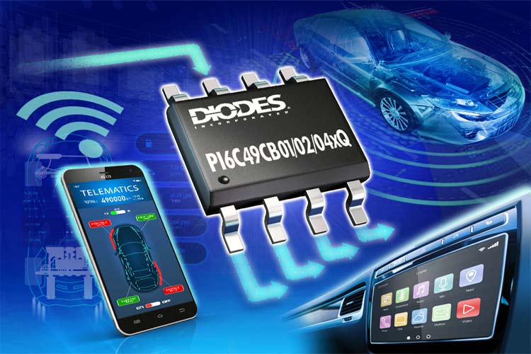
Diodes Incorporated has introduced a new family of automotive compliant clock buffers that includes the PI6C49CB01Q (one differential input, one single-ended output), PI6C49CB02Q (one single-ended input, two single-ended outputs), and PI6C49CB04xQ (one single-ended input, four single-ended outputs). These clock buffers family operates from an input voltage of between 1.5V and 3.3V and they are designed for low power CMOS operation in ambient temperatures up to 105°C, as found in advanced driver-assistance systems (ADAS), infotainment applications, and automotive gateways.
As the number of clock signals has increased in automotive electronics the demand for clock buffers that can deliver low jitter and low skew with minimum system power also increased. All the clock inputs of the new clock buffers are aligned and synchronized to maintain low skew, and the CMOS design introduces minimal phase noise, resulting in very low additive jitter.
All inputs and outputs are compatible with LVCMOS/LVTTL signal levels. The parts are qualified to AECQ-100 with full PPAP support and they are manufactured in IATF16949 certified facilities.
Features of PI6C49CB01Q
- One LVCMOS/LVTTL output
- Differential CLK/nCLK input pair
- CLK/nCLK pair can accept the following differential input levels: LVPECL, LVDS, LVHSTL, SSTL, and HCSL
- Output frequency: 360MHz
- Part-to-Part skew: 500ps (maximum)
- Additive phase jitter, RMS: 0.09ps (typical), 3.3V output
- Full 3.3V and 2.5V operating supply
- -40°C to 105°C ambient operating temperature
- AEC-Q100 Qualified
- Automotive Grade 2 temperature range (-40 to 105 °C)
- Automotive Grade 3 temperature range (-40 to 85 °C)
Features of PI6C49CB02Q
- 2 LVCMOS / LVTTL outputs
- LVCMOS / LVTTL clock input accepts LVCMOS or LVTTL input levels
- Maximum output frequency: 250MHz
- Output skew: 25ps (typical)
- Part-to-part skew: 250ps (typical)
- Small 8 lead SOIC packages save board space
- Full 3.3V, 2.5V operation modes
- AEC-Q100 Qualified
- Automotive Grade 2 temperature range (-40 to 105 °C)
- Automotive Grade 3 temperature range (-40 to 85 °C)
Note: More technical details can be found in the PI6C49CB01Q datasheet linked at the bottom of this page and in the PI6C49CB01Q, PI6C49CB02Q, and PI6C49CB04xQ product pages.


