ULN2803A - Darlington Transistor Arrays
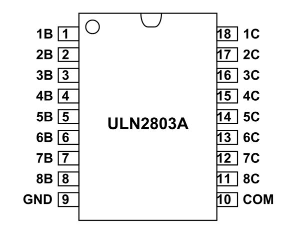
ULN2803 Pin Configuration
ULN2803 is an 18 pin IC which will be available in various packages. The description for each pin is given below.
|
Pin Number |
Description |
|
BASE CONNECTIONS for DARLINGTON ARRAYs |
|
|
1 |
1B-BASE of 1st TRANSISTOR |
|
2 |
2B- BASE of 2nd TRANSISTOR |
|
3 |
3B- BASE of 3rd TRANSISTOR |
|
4 |
4B- BASE of 4th TRANSISTOR |
|
5 |
5B- BASE of 5th TRANSISTOR |
|
6 |
6B- BASE of 6th TRANSISTOR |
|
7 |
7B- BASE of 7th TRANSISTOR |
|
8 |
8B- BASE of 8th TRANSISTOR |
|
SHARED TERMINALS |
|
|
9 |
GND- EMITTER of all TRANSISTORs |
|
10 |
COM- Common cathode (Negative) node for flyback diodes. |
|
COLLECTOR CONNECTIONS for DARLINGTON ARRAYs |
|
|
11 |
8C-COLLECTOR of 8th TRANSISTOR |
|
12 |
7C-COLLECTOR of 7th TRANSISTOR |
|
13 |
6C-COLLECTOR of 6th TRANSISTOR |
|
14 |
5C-COLLECTOR of 5th TRANSISTOR |
|
15 |
4C-COLLECTOR of 4th TRANSISTOR |
|
16 |
3C-COLLECTOR of 3rd 6thTRANSISTOR |
|
17 |
2C-COLLECTOR of 2nd TRANSISTOR |
|
18 |
1C-COLLECTOR of 1st TRANSISTOR |
ULN2803 Features and Specifications
- Maximum voltage allowed between COLLECTOR and EMITTER of each DARLINGTON TRANSISTOR: 50V
- Maximum current allowed trough COLLECTOR of each DARLINGTON TRANSISTOR: 500mA
- Maximum voltage allowed between BASE and EMITTER of each DARLINGTON TRANSISTOR: 30V
- Maximum current allowed trough FLYBACK DIODE of each DARLINGTON TRANSISTOR: 500mA
- Typical Rise Time: 130ns
- Typical Fall Time: 20us
- Operating temperature: -65°C to 150 °C
- No additional power needed to be applied for chip for making it work.
Note: Complete technical information can be found in the ULN2803 Datasheet linked at the bottom of this page.
ULN2803 Equivalent ICs
There are no PIN to PIN replacements for ULN2803 but there are similar functioning ICs like ULN2003, ULN2004. You can remodel eight DARLIGNGTON TRANSISTORS or eight MOSFETs to substitute for ULN2803.
Where to Use ULN2803 IC
For understanding the use of ULN2803 consider:
Case1: Where you need to control Inductive loads using LOGIC from CONTROL UNIT. DARLINGTON ARRAYs in ULN2803 IC simply acts as eight individual switches which can be triggered ON and OFF individually. Each set can drive a HIGH POWER LOAD taking LOGIC from CONTROL UNIT.
Case2: Where you want to drive multiple loads. ULN2803 can drive eight loads simultaneously. Although using MOSFETS or TRANSISTORs will suffice, but placing eight devices on board will becomes cumbersome. So using ULN2803 is best for replacing bulk switching devices.
Case3: Programmable LOAD SHARING. When we have one HIGH POWER LOAD and ONE LOW POWER LOAD, we can connect multiple ARRAYs parallel together to drive a HIGH POWER LOAD.
How to Use ULN2803?
As mentioned earlier ULN2803 has eight DARLIGNTON ARRAYS which acts as eight switching devices. The simplified internal structure can be given as below. Here each NOT gate represent DARLIGTON TRANSISTOR setup.
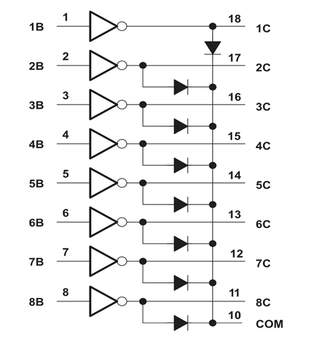
Now let’s pick one DARLIGHTON TRANSISITOR of all eight. We will have something like this:
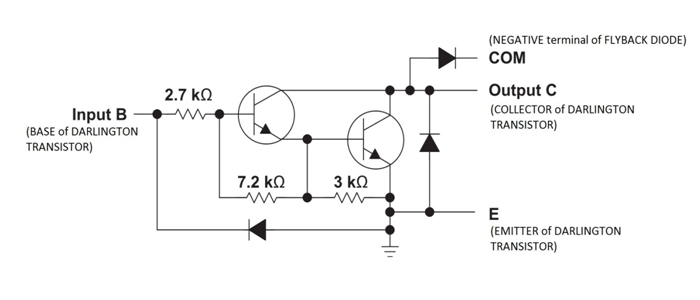
Simplified diagram of DARLIGHTON TRANSISITOR can be given as:
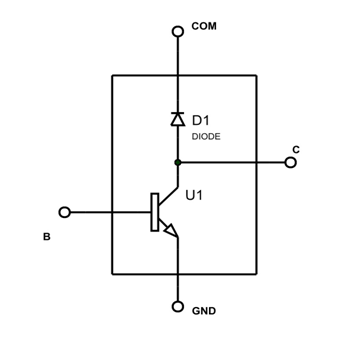
From this you can see each DARLIGHTON ARRAY can be used as single power transistor. So we can say we have eight power transistors embedded in ULN2803.
For understanding, consider the circuit:
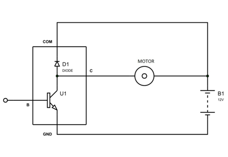
As shown in figure a MOTOR is connected to COLLECTOR of one DARLIGHTON TRANSISITOR. And the FLYBACK DIODE is connected to BATTERY POSITIVE to feedback the INDUCTIVE VOLTAGE SPIKES of MOTOR back to voltage source. GND (EMITTER) is connected to source NEGATIVE.
Under normal circumstances the MOTOR will be OFF and the complete voltage appears across the TRANSISTOR. When the BASE is provided with power the TRANSISTOR will turn ON. When the TRANSISTOR turns ON the current flows through the MOTOR following COLLECTOR and reaches ground. With current flow the MOTOR rotates.
When the BASE power is grounded, the TRANSISTOR turns OFF. With TRANSISTOR going OFF the MOTOR stops rotating.
This way we can use each set of all eight DARLIGHTON ARRAY individually.
Switching Time of ULN2803
Under normal circumstances you have no need to consider the SWITCHING DELAYS of ULN2803 IC. These delays are the response time delays of ULN2803. These delays only need to be considered when switching frequencies goes beyond 2MHz.
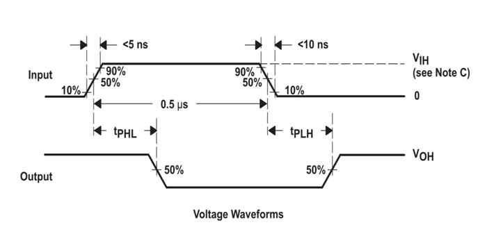
When the switching frequencies to TRANSISTOR go higher, we need to take into account the two parameters of ULN2803. These two parameters are RISETIME (tPHL) and FALLTIME (tPLH).
In the graph, VoH goes LOW when TRANSISTOR is ON and VoH goes HIGH when TRANSITOR is OFF. In another sense it is the voltage across the transistor and it represents the state of the DARLIGTON TRANSISTOR.
As in graph, consider the BASE of TRANSISTOR is provided with power. The TRANSISTOR gets turned ON, with that VoH in graph goes LOW. But as you can see in the graph there is time delay between providing LOGIC INPUT and VoH going LOW. This delay in providing response is called RISETIME (tPHL). The RISETIME (tPHL) is 130ns.
Similarly consider the BASE power is cutoff, the DARLINGTON TRANSISTOR gets turned OFF. But as you can see in the graph there is time delay between LOGIC INPUT going LOW and VoH going HIGH at the OUTPUT. This delay in providing response is called FALLTIME (tPLH ). The FALLTIME (tPLH ) is 20ns.
Total is 150ns for each cycle. These delays must be considered at higher frequencies to eliminate errors.
Applications
- Relay Drivers
- Hammer Drivers
- Lamp Drivers
- Display Drivers (LED and Gas Discharge)
- Line Drivers
- Logic Buffers
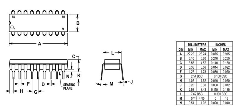
2D-Model and Dimensions