SN75176BP Bus Transceiver
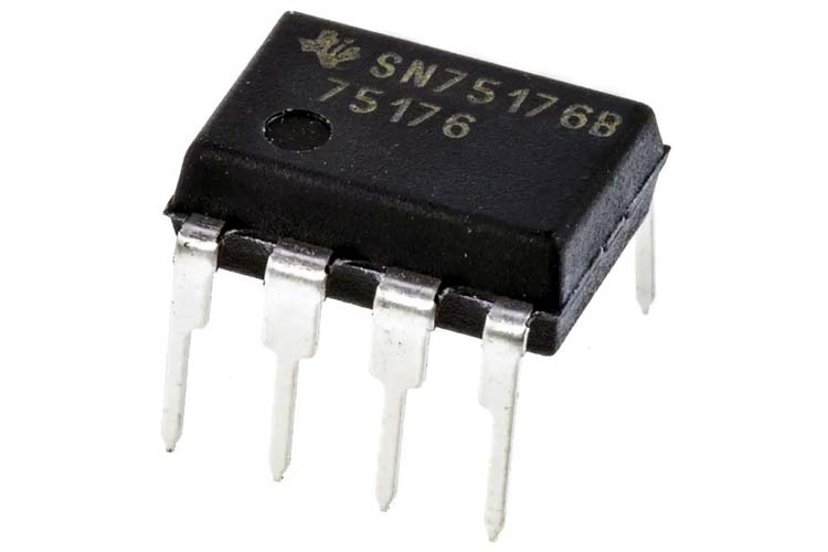
The SN75176BP is a bus transceiver that contains both transmitting and receiving circuitry for a differential bus with their respective enable circuitry. It can be used to interface with a differential data bus on protocols like RS-422 or RS-458. It is compatible with 5V logic levels.
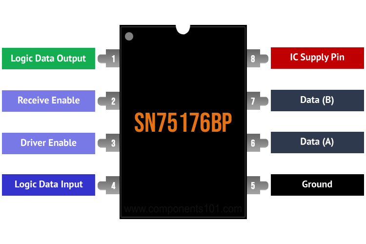
SN75176BP Pinout Description
|
Pin Number |
Pin Name |
Description |
|
1 |
R |
Logic data output |
|
2 |
|
Receive enable |
|
3 |
DE |
Driver enable |
|
4 |
D |
Logic data input |
|
5 |
GND |
IC ground reference |
|
6 |
A |
Data |
|
7 |
B |
Data |
|
8 |
VCC |
IC supply pin |

Features and Specifications
- 3-state driver and receiver outputs
- +/-60mA drive capability
- Single 5V supply
Note: Complete technical details can be found in the SN75176BP datasheet linked at the end of this page.
Equivalent
SN65176B
Other Bus Transceivers
How To Use SN75176BP
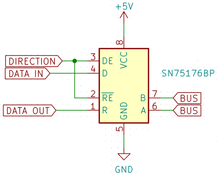
Fig. - SN75176BP Circuit
The SN75176BP from Texas Instruments is a differential bus transceiver. The name ‘transceiver’ tells us that it is both a transmitter and a receiver. The need for bussing signals arises from the fact that if there are a lot of devices that need to be connected to a central computer, the number of wires would quickly become impractical. For this reason, all the devices are connected to a common set of wires called the bus.
Since the devices connected to the bus are logic devices with logic outputs, the outputs of each device would interfere with the others. This problem can be solved with open collector outputs that can be connected together, with a pull-up resistor at the source. This scheme becomes impractical over longer distances, where large currents need to be sourced and sunk in order to maintain bandwidth and signal quality.
The SN75176BP has push-pull outputs that can be disabled, leaving the output in a high impedance state. This is accomplished by controlling each output transistor separately in such a way that either is on, or both are off. The IC has a DE (Data Enable) and a RE (Read Enable) pin that controls data direction. When the DE pin is asserted, the bus pins A and B are turned into outputs that transmit data put into the D pin. If RE is pulled low, the outputs are turned off and the A and B pins are turned into inputs. Since DE and RE pins are active high and active low respectively, they can be connected together, so when pulled low, the chip reads data from the bus, and when pulled high, writes data to the bus.
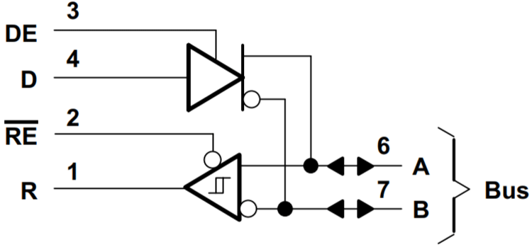
Fig. - SN75176BP Internal Circuit
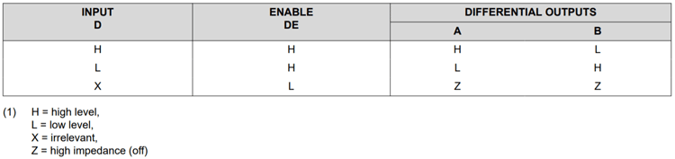
Fig. - SN75176BP Truth Table
Applications
- Motor controller
- Wireless repeaters
- Human-machine interfaces
2D Model and Dimensions
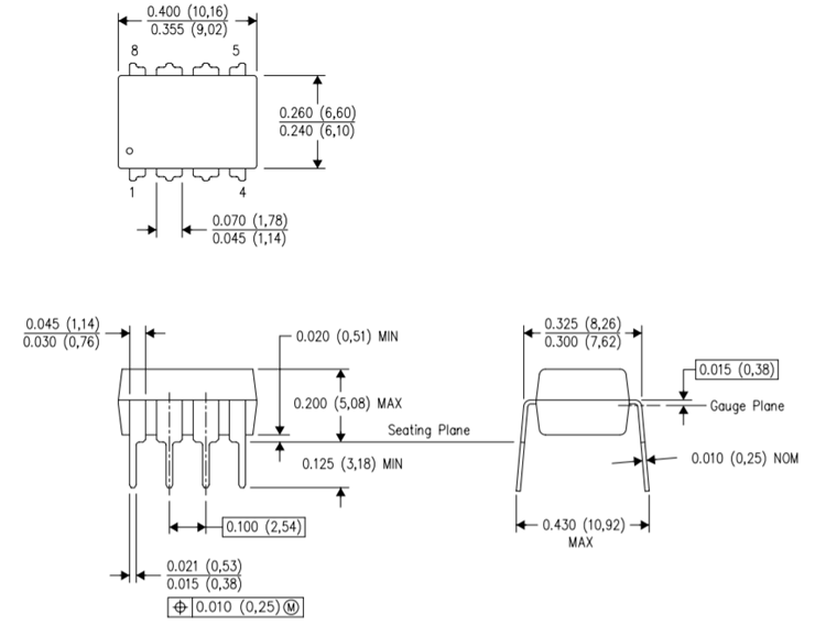
*Dimensions are in mm


