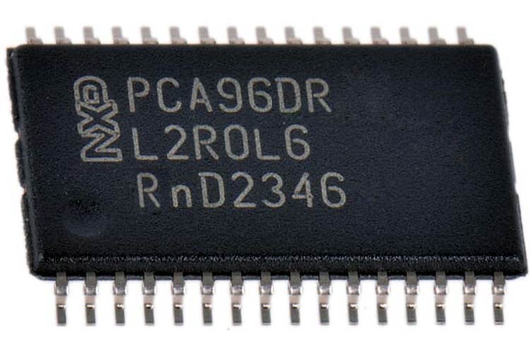
PCA9685 16-Channel, 12-bit PWM/Servo/LED Driver
The PCA9685 is an I2C-bus controlled 16-channel LED controller optimized for Red/Green/Blue/Amber (RGBA) color backlighting applications. Each LED output has its own 12-bit resolution (4096 steps) fixed frequency individual PWM controller that operates at a programmable frequency from a typical of 24Hz to 1526Hz with a duty cycle that is adjustable from 0% to 100% to allow the LED to be set to a specific brightness value. All outputs are set to the same PWM frequency.
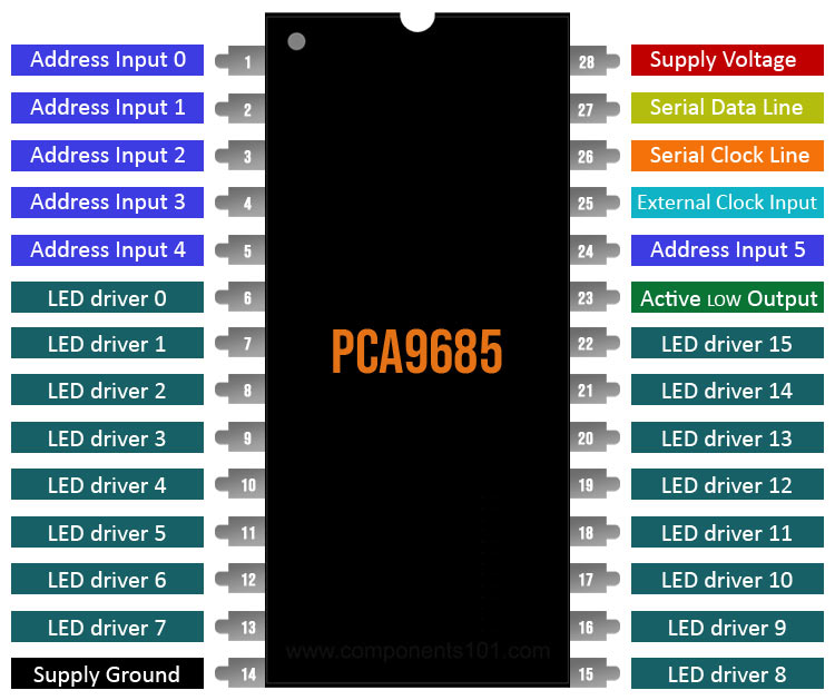
PCA9685 Pin Configuration
|
Pin No. |
Pin Name |
Pin Configuration |
|
1 |
A0 |
address input 0 |
|
2 |
A1 |
address input 1 |
|
3 |
A2 |
address input 2 |
|
4 |
A3 |
address input 3 |
|
5 |
A4 |
address input 4 |
|
6 |
LED0 |
LED driver 0 |
|
7 |
LED1 |
LED driver 1 |
|
8 |
LED2 |
LED driver 2 |
|
9 |
LED3 |
LED driver 3 |
|
10 |
LED4 |
LED driver 4 |
|
11 |
LED5 |
LED driver 5 |
|
12 |
LED6 |
LED driver 6 |
|
13 |
LED7 |
LED driver 7 |
|
14 |
Vss |
Supply Ground |
|
15 |
LED8 |
LED driver |
|
16 |
LED9 |
LED driver 9 |
|
17 |
LED10 |
LED driver 10 |
|
18 |
LED11 |
LED driver 11 |
|
19 |
LED12 |
LED driver 12 |
|
20 |
LED13 |
LED driver 13 |
|
21 |
LED14 |
LED driver 14 |
|
22 |
LED15 |
LED driver 15 |
|
23 |
OE |
active LOW output enable |
|
24 |
A5 |
address input 5 |
|
25 |
EXTCLK |
external clock input |
|
26 |
SCL |
serial clock line |
|
27 |
SDA |
serial data line |
|
28 |
VDD |
supply voltage |
Features & Specifications
- 16 LED drivers. Each output is programmable at off, on, Programmable LED brightness, and Programmable LED turn-on time to help reduce EMI
- 1 MHz Fast-mode Plus compatible I2C-bus interface with 30 mA high drive capability on SDA output for driving high capacitive buses
- 4096-step (12-bit) linear programmable brightness per LED output varying from fully off (default) to maximum brightness
- LED output frequency (all LEDs) typically varies from 24 Hz to 1526 Hz (Default of 1Eh in PRE_SCALE register results in a 200 Hz refresh rate with oscillator clock of 25 MHz.)
- Sixteen totem pole outputs (sink 25 mA and source 10 mA at 5 V) with software-programmable open-drain LED outputs selection (default at totem pole). No input function.
- Output state change programmable on the Acknowledge or the STOP Command to update outputs byte-by-byte or all at the same time (default to ‘Change on STOP’).
- Active LOW Output Enable (OE) input pin. LEDs outputs programmable to logic 1, logic 0 (default at power-up), or ‘high-impedance’ when OE is HIGH.
- 6 hardware address pins allow 62 PCA9685 devices to be connected to the same I2C-bus
- Toggling OE allows for hardware LED blinking
- 4 software-programmable I2C-bus addresses (one LED All Call address and three LED Sub Call addresses) allow groups of devices to be addressed at the same time in any combination (for example, one register used for ‘All Call’ so that all the PCA9685s on the I2C-bus can be addressed at the same time and the second register used for three different addresses so that 1/3 of all devices on the bus can be addressed at the same time in a group). The software enables and disables these I2C-bus addresses.
- Software Reset feature (SWRST General Call) allows the device to be reset through the I2C-bus
- 25 MHz typical internal oscillator requires no external components
- External 50 MHz (max.) clock input
- Internal power-on reset
- Noise filter on SDA/SCL inputs
- Edge rate control on outputs
- No output glitches on power-up
- Supports hot insertion
- Low standby current
- Operating power supply voltage range of 2.3 V to 5.5 V
- 5.5 V tolerant inputs
- -40 C to +85 C operation ESD protection exceeds 2000 V HBM per JESD22-A114, 200 V MM per JESD22-A115, and 1000 V CDM per JESD22-C101
- Latch-up testing is done to JEDEC Standard JESD78 which exceeds 100 mA
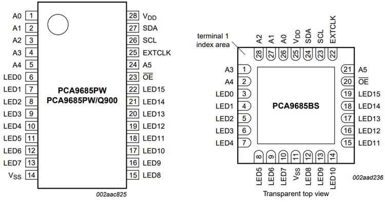
- Packages offered: TSSOP28, HVQFN28
PCA9685 Equivalents
TLC5971, LED6001, MAX16803, RT9288A
Note: Complete technical details about this IC can be found in the PCA9685 datasheet at the end of the page.
How to use PCA9685 PWM LED Controller IC
Using the PCA9685 IC is very simple as it uses an I2C bus to communicate between devices, for clarification the block diagram of the device is shown below,
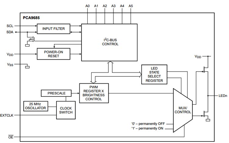
As you can see from the above image you have your SCL and SDA line for communication, which obviously you need to use two pullup resistors as the device does not feature internal pullup resistors. Also, you have your A0 to A5 address lines that are used to set the I2C address of the device, the device also has the option to operate the with external clock or we can do that with an internal clock. For more information on I2C, its addresses and other requirements do checkout the datasheet linked down below.
Applications
- RGB or RGBA LED drivers
- LED status information
- LED displays
- LCD backlights
- Keypad backlights for cellular phones or handheld devices
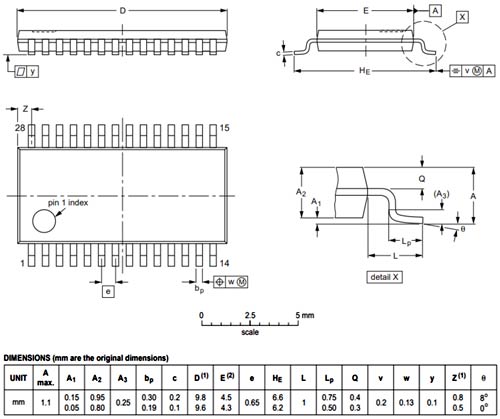
2D Model and Dimensions
If you are designing a PCB with this component then the following picture from the Datasheet will be useful to know its package type and dimensions.