LNK626PG AC-DC converter with Primary-side Constant-Voltage Control
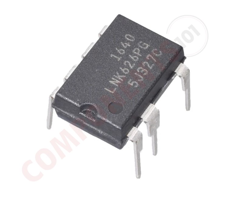
The LNK623-626 is an offline switcher IC designed to simplify the switched mode power supply design by eliminating the need for an optocoupler and secondary CV control circuitry. It features a very accurate primary-side Constant-Voltage (CV) control. With its innovative control technique, it ensures precise output voltage regulation while reducing component count and cost. Featuring a 725 V power MOSFET, ON/OFF control, self-biasing, and advanced protection features such as cycle-by-cycle current limit and thermal shutdown, it offers reliable performance. Additionally, it boasts eco-friendly features such as low no-load consumption and compliance with global energy efficiency regulations. Ideal for various applications, including DVDs and set-top boxes, this IC provides efficient power management solutions. The LNK626 is available in both PDIP-8C and SO-8C packages.
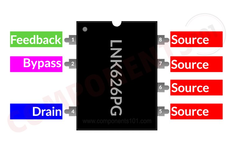
LNK626 Pinout Configuration
Here we have only included the pinout details for the PDIP and SO packages. You can get the pinout details of other packages from the datasheet attached to the end of this page.
|
NAME |
PIN |
DESCRIPTION |
|
Feedback |
1 |
During normal operation, switching of the power MOSFET is controlled by this pin. This pin senses the AC voltage on the bias winding. This control input regulates the output voltage based on the flyback voltage of the bias winding. |
|
Bypass |
2 |
Connection point for an external bypass capacitor |
|
Drain |
4 |
Power MOSFET drain pin |
|
Source |
5,6,7,8 |
The pin is internally connected to the output MOSFET source for high-voltage power return and control circuit common. |
How to identify the LNK626PG part number
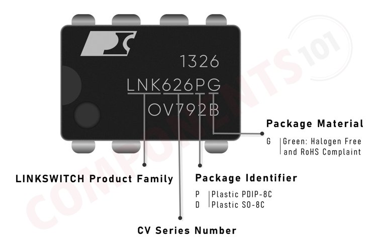
The LNK626PG is available in different packages. You can identify them using the package marking. You can find the LNK626PG with the following markings, LNK626PG and LNK626DG. The first letter after LNK626 indicates the package type and the second letter indicates ROHS compliant. For example, the PDIP or through-hole version of the IC LNK626 will have the package markings LNK626PG, while the LNK626 SMD variant will have markings like LNK626DG.
Manufacturers of LNK626PG IC:
The LNK626PG SMPS IC is manufactured by Power Integrations, under their TinySwitch II series of ICs. There are no alternative manufacturers for the same part number as of the date of writing this article.
Features of LNK626 AC-DC Converter IC:
- Eliminates optocoupler and all secondary CV control circuitry
- Eliminates bias winding supply – IC is self-biasing
- Compensates for external component temperature variations
- Very tight IC parameter tolerances using proprietary trimming technology
- Continuous and/or discontinuous mode operation for design flexibility
- Frequency jittering greatly reduces EMI filter cost
- Even tighter output tolerances achievable with external resistor selection/trimming
- Auto-restart protection reduces delivered power by >95% for output short-circuits and all control loop faults (open and shorted components)
- Hysteretic thermal shutdown – automatic recovery reduces power supply returns from the field
- Meets HV creepage requirements between the Drain and all other pins, both on the PCB and the package
- No-load consumption <200 mW at 230 VAC and down to below 70 mW with optional external bias
- Easily meets all global energy efficiency regulations with no added components
- ON/OFF control provides constant efficiency down to very light loads – ideal for mandatory EISA and ENERGY STAR 2.0 regulations
- No primary or secondary current sense resistors – maximizes efficiency
LNK626PG Equivalents
If you are looking for an equivalent or replacement for LNK626 you can look at the other IC from the same family. The only difference between them will be the maximum power rating. You can use the following table to select a proper one.
LNK626PG Alternatives
Viper22A, LNK306PN, AP3983, VIPER12A, AP8012, TNY280
Note: Complete technical details can be found in the LNK626PG datasheet at this page’s end.
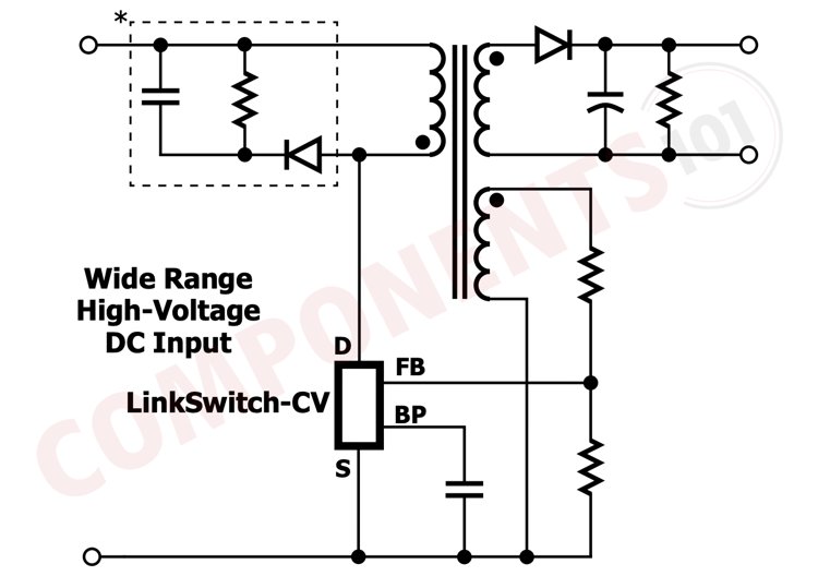
LNK626PG Schematics
The following image shows the typical LNK626PG circuit diagram.
As you can see the circuit is very simple and only requires bare minimum components. The circuit shown below is for a low-cost, high-efficiency, 7 W (10 W peak) Multiple Output Flyback Converter for DVD Applications with Primary Sensed Feedback.
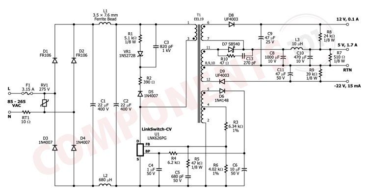
The primary side prediction includes the fuse, thermistor and an inrush current limit resistor.AC input power is rectified by diodes D1 through D4. The rectified DC is filtered by the bulk storage capacitors C1 and C2. These capacitors form a pi filter in combination with the inductors to attenuate any differential-mode EMI noise. The output side contains the rectifier and filter circuits for each voltage output. The LNK626 regulates the output using ON/OFF control, enabling or disabling switching cycles based on the sampled voltage on the FEEDBACK pin. The output voltage is sensed using a primary referenced winding on transformer T1 eliminating the need for an optocoupler and a secondary sense circuit.
Design Tips for LNK626 IC
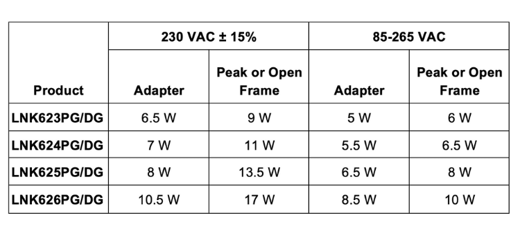
What's the maximum power that we can get from a LNK626 SMPS?
It will depend on the construction, and form an adapter type, ie from an enclosed power supply we can get up to 10.5W power for a fixed 230 VAC input and 8.5W for universal input(85-265 VAC). From an open-frame power supply, we can get 17W power for the fixed input voltage of 230 VAC and 10W for universal input(85 -265 VAC).
Do we need an external MOSFET with LNK626?
No, we don’t. The LNK626 feature an integrated power MOSFET.
What are the design considerations when designing an LNK626 power supply PCB.
When designing a board for the LNK626-based power supply, adhere to the following guidelines:
- Single Point Grounding: Utilize a single point (Kelvin) connection at the negative terminal of the input filter capacitor for the LinkSwitch-CV SOURCE pin and bias winding return to enhance surge capabilities.
- Bypass Capacitor: Position the BYPASS pin capacitor as close as possible to the SOURCE and BYPASS pins to optimize performance.
- Feedback Resistors: Directly place the feedback resistors at the FEEDBACK pin of the LinkSwitch-CV device to minimize noise coupling.
- Thermal Considerations: Connect the copper area to the SOURCE pins to act as the LinkSwitch-CV heat sink. Ensure adequate copper area to keep the SOURCE pin temperature below 110°C, considering part-to-part RDS(ON) variation.
- Secondary Loop Area: Minimize the area of the loop connecting the secondary winding, output diode, and output filter capacitor to reduce leakage inductance and EMI. Provide sufficient copper area at the anode and cathode terminal of the diode for heat sinking, with a larger area preferred at the cathode terminal.
- Electrostatic Discharge Spark Gap: In chargers and adapters, consider adding a spark gap to mitigate ESD discharges. Form one electrode of the spark gap with a trace along the isolation barrier, with the other electrode on the secondary side formed by the output return node. Place a 10 mil gap near the AC input and space the trace from the AC input to the spark gap electrode away from other traces to prevent unwanted arcing and possible circuit damage.
Troubleshooting Tips for LNK626PG
Here are some troubleshooting tips for dealing with issues related to the LNK626PG:
No Output Voltage or Power Supply Not Starting:
- Ensure the input power is connected and within the specified range for the LNK626PG.
- A blown fuse or faulty rectifier diode can prevent the circuit from powering up.
- Double-check all component values, especially feedback resistors, to ensure they are within the specified range.
Overheating or Thermal Shutdown:
- Ensure sufficient cooling for the IC. Overheating can result from inadequate heat sinking or poor airflow.
- Overloading the power supply can cause excessive heat. Ensure the load is within the IC's specified limits.
- Look for any potential short circuits on the output side that might cause excessive current draw.
Unstable Output Voltage:
- Ensure the feedback loop is correctly designed, and components are not defective. Incorrect feedback can lead to unstable output.
- Low-quality or degraded capacitors can cause instability. Check for capacitors with low ESR values.
Excessive Noise or Ripple:
- Filter Capacitors: Verify that the input and output filter capacitors are of adequate value and quality.
- Layout Issues: Poor PCB layout can contribute to noise. Ensure trace lengths are minimized, and high-current paths are properly routed.
Underperformance in Load Regulation:
- Check Output Load: Ensure the load is within the IC's capabilities.
- Feedback Resistor Values: Incorrect feedback resistor values can affect load regulation.
Electromagnetic Interference (EMI) Issues:
- Ensure good PCB layout practices to minimize EMI.
- Proper shielding and grounding techniques can help reduce EMI.
Unexpected Resets or Shutdowns:
- Transient voltage spikes can cause resets. Check with an oscilloscope for any abnormal spikes.
- Overheating can cause similar issues. Check if the chip is with in the rated temperature using non-contact thermometers or thermal cameras.
Applications of LNK626:
● DVD/STB
● Adapters
● Standby and auxiliary supplies
● Home appliances, white goods and consumer electronics
● Industrial controls
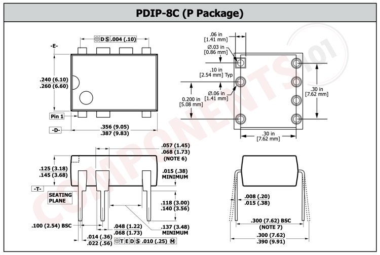
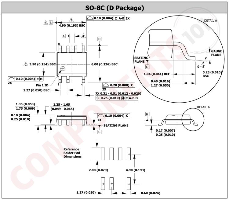
2D-Model and Dimensions:
Below is the 2D CAD drawing of LNK626 along with its dimensions. The dimensions can be used to create custom footprints of the module and be used for PCB or CAD modelling.