HX710B - 24-Bit ADC for Weighing Scale Applications
The HX710B is a precision 24-bit analog-to-digital converter (ADC) designed for weigh scales and industrial control applications. It offers direct interface capabilities with a bridge sensor and DVDD, AVDD voltage difference detection. The ADC's input stage features a low-noise amplifier with a fixed gain of 128, corresponding to a full-scale differential input voltage of ±20mV when a 5V reference voltage is connected to the VREF pin. To simplify the digital interface initialization, the device incorporates on-chip power-on-reset circuitry. Additionally, the HX710 includes an on-chip oscillator that provides the necessary system clock without the need for external components. The internal registers of the device do not require any programming, as all controls are managed through the available pins. Even though it is designed for weighing scale applications, you can find them in many other sensing circuitries such as pressure sensor and more.
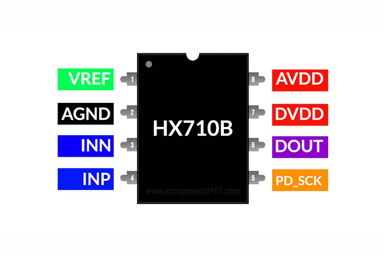
HX710B Pinout Configuration
|
Pin |
Name |
Function |
Description |
|
1 |
VREF |
Analog Input |
Reference input voltage: 1.8 ~ 5.5V |
|
2 |
AGND |
Ground |
Analog Ground |
|
3 |
INN |
Analog Input |
Differential signal negative input |
|
4 |
INP |
Analog Input |
Differential signal positive input |
|
5 |
PD_SCK |
Digital Input |
Power down control (high active) and serial clock input |
|
6 |
DOUT |
Digital Output |
Serial data output |
|
7 |
DVDD |
Power |
Digital supply: 2.6 ~ 5.5V |
|
8 |
AVDD |
Power |
Analog supply: 2.6 ~ 5.5V |
Features
- DVDD and AVDD supply voltage difference measurement
- On-chip low noise amplifier with a gain of 128
- On-chip oscillator requiring no external Component
- On-chip power-on-reset
- Simple digital control and serial interface: pin-driven controls, no programming needed.
- Selectable 10SPS or 40SPS output data rate
- Simultaneous 50 and 60Hz supply rejection
- Current consumption: normal operation < 1.2mA, power down < 1uA
- Operation supply voltage range: 2.6 ~ 5.5V
- Operation temperature range: -40 ~ +85 °C
- 8 pin SOP-8 package.
Other Popular ADCs
HX711, MCP3008, ADS1115, ADC0804
Note: Complete technical details can be found in the HX710B datasheet at this page’s end.
Application Circuit
The following image shows the typical application circuit for the HX710B.
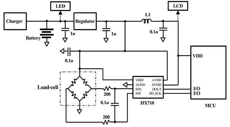
In HX710B, the on-chip oscillator serves as the clock source. The nominal output data rate for this version is either 10 or 40 samples per second. It is essential to ensure that the digital power supply (DVDD) matches the power supply of the microcontroller unit (MCU). Additionally, the analog power supply (AVDD) should not exceed the digital supply (DVDD). For the A/D conversion reference voltage (VREF), it should be connected to the supply voltage of the load cell. This connection can be made directly to AVDD or through a resistor to reduce power consumption by the load cell.
The data retrieval, input selection, output data rate selection, and power down controls of the HX710B utilize the PD_SCK and DOUT pins. When the output data is not yet ready for retrieval, the digital output pin DOUT remains in a high state, while the serial clock input PD_SCK should be low. Once the data becomes available for retrieval, DOUT transitions to a low state. To retrieve the data, 25~27 positive clock pulses are applied to the PD_SCK pin. The data is then shifted out from the DOUT output pin, with each PD_SCK pulse shifting out one bit in a sequence starting from the most significant bit (MSB) until all 24 bits have been shifted out. When the 25th pulse is applied to the PD_SCK input, the DOUT pin returns to a high state.
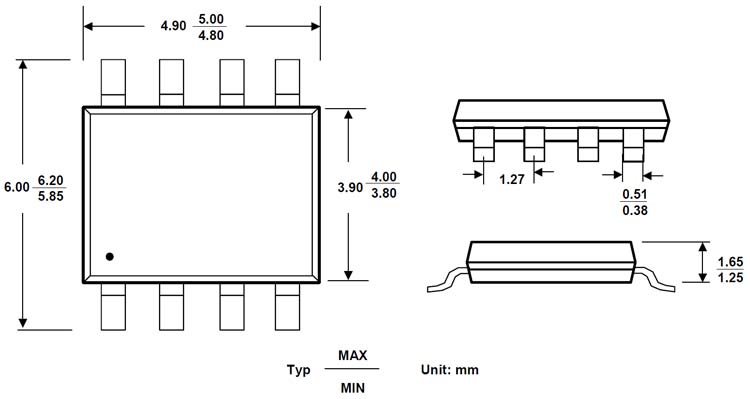
2D-Model and Dimensions
Below is the 2D CAD drawing of HX710B ADC along with its dimensions in millimetres. The dimensions can be used to create custom footprints of the module and be used for PCB or CAD modeling.