FDC1004 4-Channel Capacitive Sense IC
The FDC1004 is a 4-channel capacitance-to-digital converter. Which is designed to fabricate capacitance-sensing devices or modules. Each channel can accurately measure capacitance changes within the ±15 pF range. if the sensor has an offset capacitance of up to 100 pF, the FDC1004 can accurately measure changes in capacitance relative to this offset. The FDC1004 can compensate for this offset in its measurements. Alternatively, an external capacitor can be used to track environmental changes over time and temperature, which will help measure accurate capacitance in varying conditions. The FDC1004 comes with shield drivers for sensor shields, which will significantly reduce the EMI interference. We can communicate between the FDC1004 and the microcontroller through the I2C protocol. The FDC1004 comes in 10-pin WSON and VSSOP packages, so these small footprints of the FDC1004 help to build small modules and devices. This chip is widely used in Proximity Sensor, Gesture Recognition and Automotive Doors.
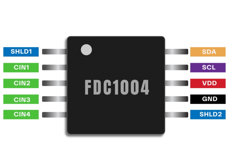
FDC1004 Pinout Configuration
Here are the pinout details for FDC1004.
| PIN NO | PIN NAME | DESCRIPTION |
| 1 | SHLD1 | Capacitive Input Active AC Shielding. |
| 2 | CIN1 | Capacitive Input. The measured capacitance is connected between the CIN1 pin and GND. If not used, this pin should be left as an open circuit. |
| 3 | CIN2 | Capacitive Input. The measured capacitance is connected between the CIN2 pin and GND. If not used, this pin should be left as an open circuit. |
| 4 | CIN3 | Capacitive Input. The measured capacitance is connected between the CIN3 pin and GND. If not used, this pin should be left as an open circuit. |
| 5 | CIN4 | Capacitive Input. The measured capacitance is connected between the CIN4 pin and GND. If not used, this pin should be left as an open circuit. |
| 6 | SHLD2 | Capacitive Input Active AC Shielding. |
| 7 | GND | Ground |
| 8 | VDD | Power Supply Voltage. This pin should be decoupled to GND, using a low impedance capacitor, for example in combination with a 1-μF tantalum and a 0.1-μF multilayer ceramic. |
| 9 | SCL | Serial Interface Clock Input. Connects to the master clock line. Requires pull-up resistor if not already provided elsewhere in the system. |
| 10 | SDA | Serial Interface Bidirectional Data. Connects to the master data line. Requires a pull-up resistor if not provided elsewhere in the system. Connect to GND |
Manufacturers of FDC1004:
FDC1004 4-Channel Capacitance-to-Digital Converter is manufactured only by Texas Instruments
FDC1004 Equivalents
There aren't any pin-to-pin compatible equivalents available for FDC1004. You may check out FDC2214, which has the same function but with more resolution. But it is also available in a different package than FDC1004.
FDC1004 Alternatives
If you are looking for an alternative for FDC1004 you can look at the other IC from these.
AD7745, AD7746M, MCP3910A, MAX14720, FDC2214, TTP229, TTP224, TTP223, TTP226
Note: Complete technical details can be found in the FDC1004 datasheet at this page’s end.
Features of FDC1004
FDC1004 is a 4-channel capacitance-to-digital converter (CDC) with the following key features:
- Precise Capacitance Measurement down to femtofarad (fF) levels
- 4-Channel Input: The FDC1004 can monitor up to four capacitive sensors simultaneously
- High Resolution: up to .5fF
- Low Power Consumption: The FDC1004 is designed for low-power operation, making it suitable for battery-powered applications.
- I2C Interface: It communicates with a microcontroller or host device via I2C, providing easy integration into digital systems.
- Small Form Factor: The FDC1004 is available in a small, space-saving package, making it suitable for applications with size constraints.
FDC1004 Schematics
The following image shows the typical FDC1004 application (Liquid Level Measurement) circuit diagram.
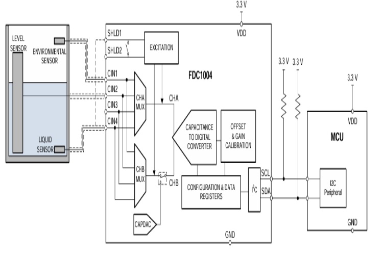
The liquid level measurement should be independent of the liquid, which can be achieved using the 3-electrode design described above. Moreover, the sensor should be immune to environmental interference such as the human body, other objects, or EMI. This can be achieved by shielding the side of the sensor which does not face the container.
In capacitive sensing systems, the design of the sensor plays an important role in determining system performance and capabilities. In most cases, the sensor is simply a metal plate that can be designed on the PCB. The sensor used in this example is implemented with a two-layer PCB. On the top layer, which faces the tank, there are the 3 electrodes (Reference Environmental, Reference Liquid, and Level) with a ground plane surrounding the electrodes. The bottom layer is covered with a shield plane in order to isolate the electrodes from any external interference sources. Depending on the shape of the container, the FDC1004 can be located on the sensor PCB to minimize the length of the traces between the input channels and the sensors and increase the immunity from EMI sources. In case the shape of the container or other mechanical constraints do not allow having the sensors and the FDC1004 on the same PCB, the traces which connect the channels to the sensor need to be shielded with the appropriate shield. In this design example, all of the channels are shielded with SHLD1. For this configuration, the FDC1004 measures the capacitance of the 3 channels versus ground; and so the SHLD1 and SHLD2 pins are internally shorted in the FDC1004.
Troubleshooting Tips for FDC1004
- Power Supply: Ensure that the power supply to the FDC1004 is stable and within the specified voltage range. Check for any voltage drops or fluctuations that could affect the device's operation.
- Temperature Compensation: If you are using temperature compensation, ensure that the temperature sensor is working correctly, and that the compensation algorithm is properly implemented.
- Capacitive Gain Calibration: The gain is factory calibrated up to ±15 pF in the production for each part individually. The factory gain coefficient is stored in a one-time programmable (OTP) memory. The gain can be temporarily changed by setting the Gain Calibration Register (registers 0x11 to 0x14) for the appropriate CINn pin, although the factory gain coefficient will be restored after power-up or reset. The part is tested and specified for use only with the default factory calibration coefficient. Adjusting the Gain calibration can be used to normalize the capacitance measurement of the CINn input channels.
- Capacitive System Offset Calibration: The capacitive offset can be due to many factors including the initial capacitance of the sensor, parasitic capacitances of board traces, and the capacitance of any other connections between the sensor and the FDC. The parasitic capacitances of the FDC1004 are calibrated out at production. If there are other sources of offset in the system, it may be necessary to calibrate the system capacitance offset in the application. Any offset in the capacitance input larger than ½ LSB of the CAPDAC should first be removed using the on-chip CAPDACs. Any residual offset of approximately 1 pF can then be removed by using the capacitance offset calibration register. The offset calibration register is reloaded by the default value at power-on or after reset. Therefore, if the offset calibration is not repeated after each system power-up, the calibration coefficient value should be stored by the host controller and reloaded as part of the FDC1004 setup.
Design tips for FDC1004
1. Is the distance between the sensor and FDC1004 will affect the performance?
Yes. Avoid long traces to connect the sensor to the FDC1004. Short traces reduce parasitic capacitances between shield versus input channel and parasitic resistance between input channel versus GND and shield versus GND.
2. How to protect the sensor from short circuits?
Since the sensor in many cases is simply a metal surface on a PCB, it needs to be protected with solder resist to avoid short circuits and limit any corrosion. Any change in the sensor may result in a change in system performance.
3. What are the design considerations when designing a PCB using FDC1004?
The FDC1004 measures the capacitances connected between the CINn (n=1..4) pins and GND. To get the best result, locate the FDC1004 as close as possible to the capacitive sensor. Minimize the connection length between the sensor and FDC1004 CINn pins and between the sensor ground and the FDC1004 GND pin. If a shielded cable is used for remote sensor connection, the shield should be connected to the SHLDm (m=1...2) pin according to the configured measurement.
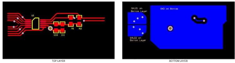
Below is optimized for applications where the sensor is not too far from the FDC1004. Each channel trace runs between 2 shield traces. This layout allows the measurements of 4 single-ended capacitance or 2 differential capacitances. The ground plane needs to be far from the channel traces, it is mandatory around or below the I2C pin.
Applications of FDC1004
- Proximity Sensor
- Gesture Recognition
- Automotive Door / Kick Sensors
- Automotive Rain Sensor
- Remote and Direct Liquid Level Sensor
- High-resolution Metal Profiling
- Rain / Fog / Ice / Snow Sensor
- Material Size Detection
- Material Stack Height
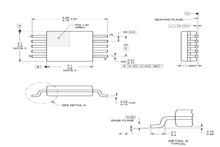
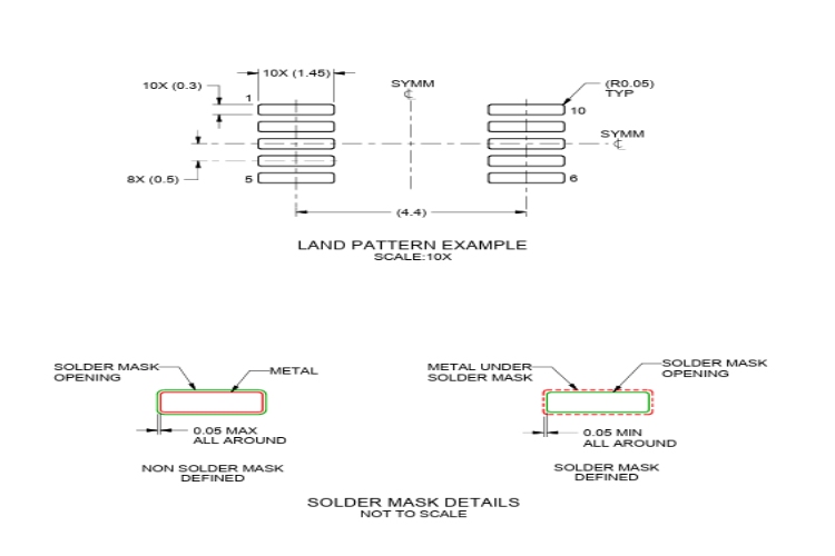
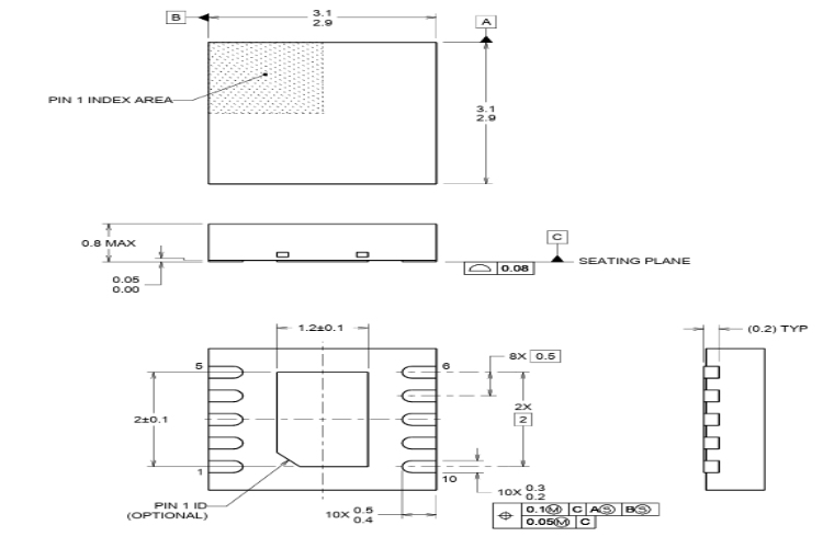
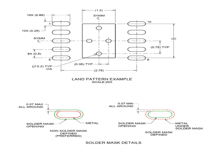
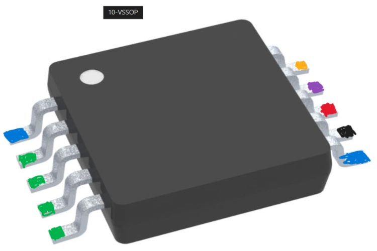
2D model and dimensions of FDC1004
Here you can find the mechanical drawings of FDC1004 along with its dimensions. The dimensions can be used to create custom footprints of the module and be used for PCB or CAD modelling.