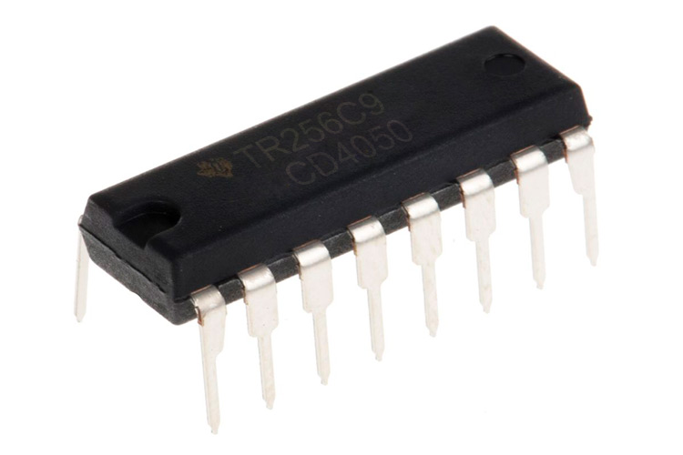
CD4050 Hex Buffer Non-Inverter IC
CD4050 IC is a hex buffer IC consists of six individual non-inverting buffers. The IC can be used to drive up to two DTL or TTL devices at a time. The IC can be used as hex buffers, CMOS current drivers or as CMOS to DTL/ TTL converters.
Features and Specification
This section mentions some of the features and specifications of the Up counter IC.
- Operating Voltage: 3V - 15V DC
- Current consumption(max): 50mA
- High Sink Current for Driving 2 TTL Loads
- Maximum low-level output Voltage: 0.5V at 5V Vcc
- Minimum high-level output voltage: 4.95 at 5V Vcc
Note: More technical information can be found in the CD4050 Datasheet, linked at the bottom of this page.
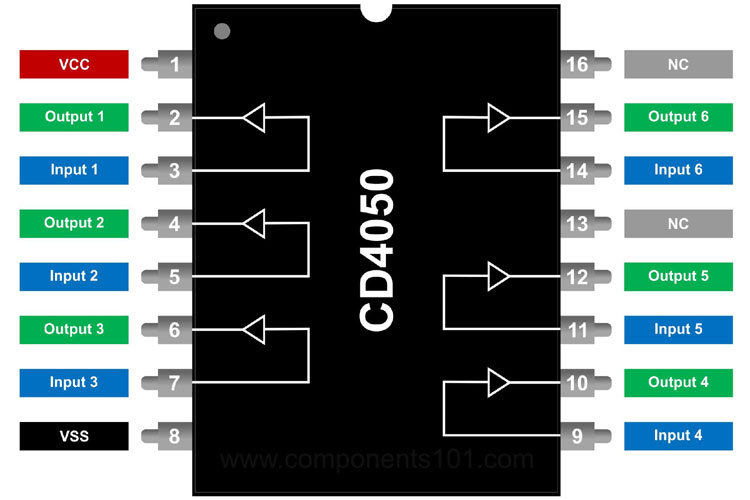
CD4050 Pinout Configuration
The non-inverting IC consists of 16 pins for I/O and power. The table below can be referred to understand the pin configuration of the IC.
|
Pin Number |
Pin Type |
Description/Direction |
|
1 |
VCC |
Positive input supply |
|
2 |
G |
Non-Inverted output 1 |
|
3 |
A |
Input 1 |
|
4 |
H |
Non-Inverted output 2 |
|
5 |
B |
Input 2 |
|
6 |
I |
Non-Inverted output 3 |
|
7 |
C |
Input 3 |
|
8 |
VSS |
Negative Supply |
|
9 |
D |
Input 4 |
|
10 |
J |
Non-Inverted output 4 |
|
11 |
E |
Input 5 |
|
12 |
K |
Non-Inverted output 5 |
|
13 |
NC |
No connection |
|
14 |
F |
Input 6 |
|
15 |
L |
Non-Inverted output 6 |
|
16 |
NC |
No connection |
Working and Use of a Non-Inverter IC
A non-inverting buffer IC consists of non-inverters that pass the input unchanged to its output. The Non-inverter works in the opposite way of the inverter IC. The IC’s main purpose is to regenerate the input, using a strong HIGH and a strong LOW.
A non-inverting buffer has only one input and only one output and the output is equal to the input. They can be used to produce and increase the propagation delay in a circuit. The image above shows the pin configuration of the IC.
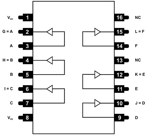
CD4050 IC Internal Schematic and Truth Table
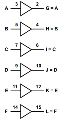
The image below shows how the non-inverting buffers are present in the IC and to which pins. As mentioned earlier, the output is always equal to the input; therefore, input to A(pin 3) will be equal to the output at G (pin 2). Similarly, the outputs will be H=B, I=C, J=D, K=E, L=f.
The table below is the truth table of the CD4050 Hex buffer IC. The input and the output of the non-inverter IC are equal.
|
Input Signal (A,B,C,D,E,F) |
Output Signal(G,H,I,J,K,L) |
|
HIGH |
HIGH |
|
LOW |
LOW |
Available Packages
SOIC, PDIP, CDIP
Applications
Here are some of the applications of the Non-Inverter IC.
- HIGH to LOW logic level converter
- DTL or TTL Hex Converters
- As CMOS current “sink” or “source” driver
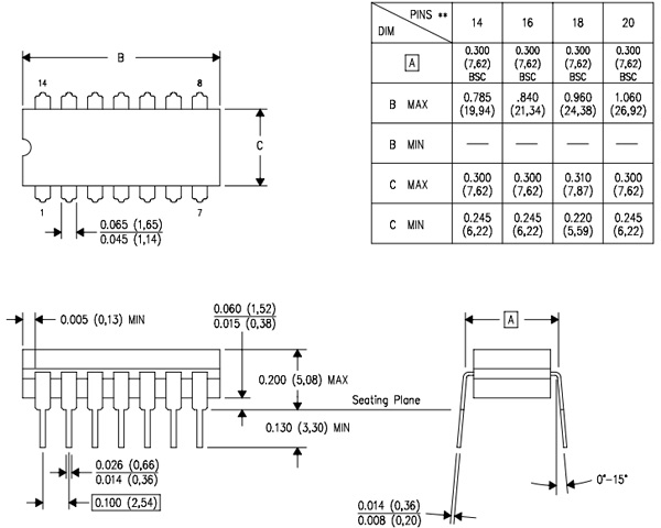
2D Model
Below is the 2D model of the Non-Inverting IC along with its dimensions in millimeters and inches. The following information can be used to design custom footprints of the IC and can be used for PCB designing and CAD modelling.