AD736 True RMS-to-DC Converter IC
The AD736 is a low-power, precision, monolithic True RMS-to-DC converter IC. It is laser trimmed to provide a maximum error of ±0.3 mV ± 0.3% of reading with sine wave inputs. Furthermore, it maintains high accuracy while measuring a wide range of input waveforms, including variable duty-cycle pulses and TRIAC (phase)-controlled sine waves. The low cost and small size of this converter make it suitable for upgrading the performance of non-RMS precision rectifiers in many applications.
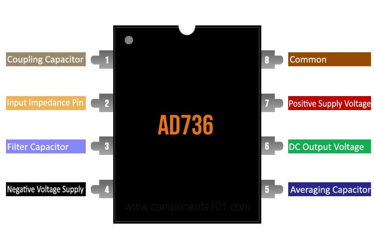
AD736 Pinout Configuration
|
Pin Number |
Pin Name |
Description |
|
1 |
CC |
Coupling Capacitor |
|
2 |
Vin |
High Input Impedance Pin |
|
3 |
CF |
Connect an Auxiliary Low-Pass Filter Capacitor from the Output |
|
4 |
-VS |
Negative Supply Voltage if Dual Supplies Are Used, or Ground if Connected to a Single-Supply Source. |
|
5 |
CAV |
Connect the Averaging Capacitor Here. |
|
6 |
OUTPUT |
DC Output Voltage. |
|
7 |
+VS |
Positive Supply Voltage. |
|
8 |
COM |
Common. |
Features & Specifications
- High input impedance: 1012 Ω
- Low input bias current: 25 pA
- maximum High accuracy: ±0.3 mV ± 0.3% of reading
- RMS conversion with signal crest factors up to 5
- Wide power supply range: +2.8 V, −3.2 V to ±16.5 V
- Low power: 200 µA maximum supply current
- Buffered voltage output
- No external trims are needed for specified accuracy
- Standby current of only 25 μA
- Output impedance is 8 kΩ
- ESD Rating 500V
- Storage Temperature Range –65°C to +150°C
Note: Complete technical details can be found in the AD736 Datasheet linked at the bottom of this page.
AD736 Equivalent ICs
AD637, AD636
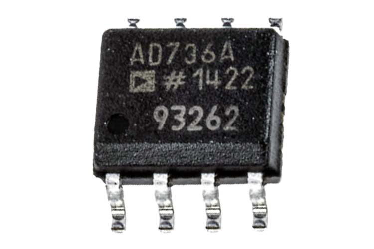
Available Packages for AD736 IC
8-Lead PDIP, 8-Lead CERDIP, 8-Lead SOIC
How to use AD736 True RMS to DC Converter IC
RMS is the abbreviation of Root Mean Square. By definition, for alternating electric current, the RMS value is equivalent to a DC voltage that puts the same amount of power into a resistor. The internal block diagram of the IC is given below.
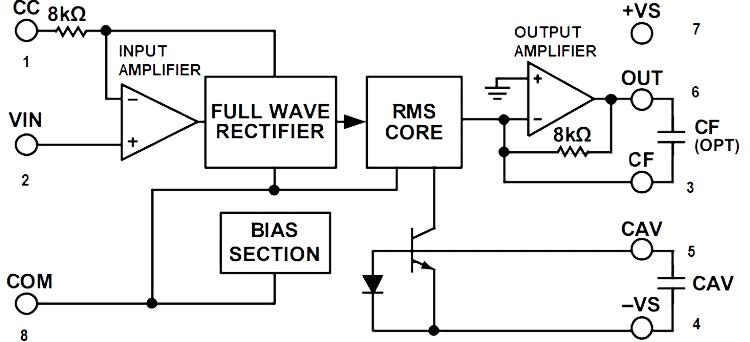
The AD736 IC has a few functional subsections like the input amplifier, full-wave rectifier, RMS core, output amplifier, and bias section. The Input amplifier is constructed with MOSFETs and is responsible for the high impedance of this IC. After the input amplifier, there is a precision full-wave rectifier that is responsible for driving the RMS core. The essential RMS operations of squaring, averaging, and square rooting are performed in the core with the help of an external averaging capacitor CAV. Finally, an output amplifier buffers the output from the RMS core and allows optional low-pass filtering to be performed via external capacitor CF, which is connected across the feedback path of the amplifier.
The AD736 IC is capable of measuring ac signals by operating as either an average responding converter or a true RMS-to-DC converter. As its name implies, an average responding converter computes the average absolute value of an ac (or ac and dc) voltage or current by full-wave rectifying and low-pass filtering the input signal; this approximates the average. The resulting output, a dc average level, is scaled by adding (or reducing) gain. This scale factor converts the dc average reading to RMS equivalent value for the waveform being measured. For example, the average absolute value of a sine wave voltage is 0.636 times VPEAK. The corresponding RMS value is 0.707 × VPEAK. Therefore, for sine wave voltages, the required scale factor is 1.11 (0.707/0.636).
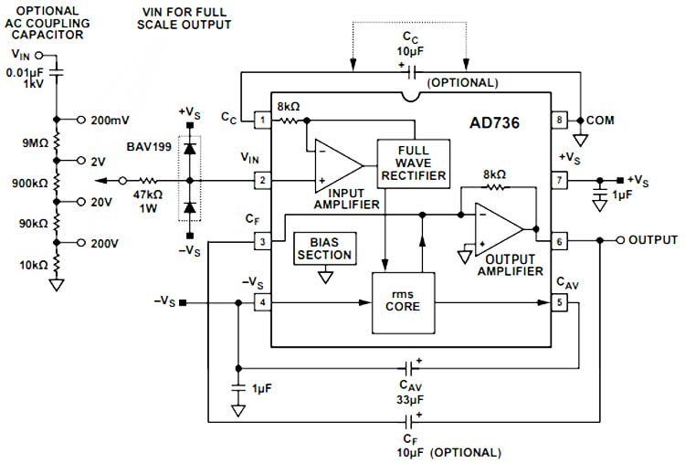
In the above figure, a simple AD736 based True RMS to DC converter circuit is shown as a multitap attenuator network used in various types of instruments requiring wide ranges of voltages. For a direct network connection, the gate-charge bleeding resistor is not required. The impedance of the FET input is high enough (1012 Ω) so that the loading error is negligible. The voltages shown in the diagrams are the input levels corresponding to 200 mV at each tap. Finally, the 47kΩ, 1 W resistor, and diode pair are a practical input protection scheme for ac line connection measurements. There are many use cases for this IC and by adding and removing a few external components, this IC can do much more, and for that do check out the datasheet linked below in the description.
Applications
- High precision non-sinusoidal voltage measurement.
- High precision Voltmeters and Multimeter.
- Battery Powered RMS to DC Conversion
- AD736 Average Responding Circuit
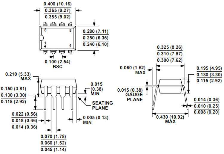
2D Model and Dimensions
If you are designing a PCB or Perf board with this component then the following picture from the Datasheet will be useful to know its package type and dimensions.