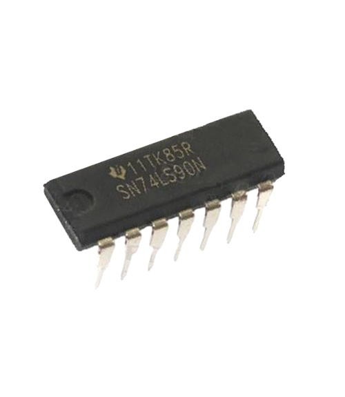
74LS90 BCD Counter IC
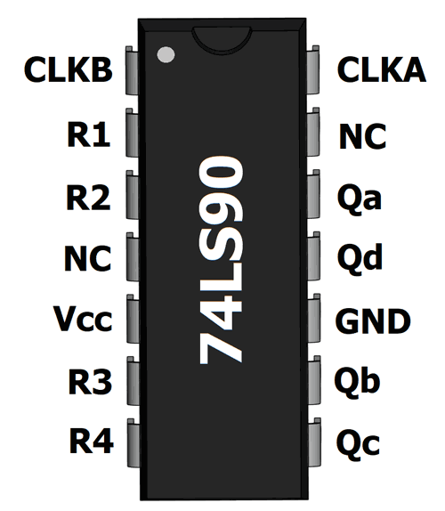
74LS90 Pin Configuration
|
Pin No. |
Pin Name |
Description |
|
1 |
CLKB |
Clock Input 2 |
|
2 |
R1 |
Reset 1 |
|
3 |
R2 |
Reset 2 |
|
4 |
NC |
Not Connected |
|
5 |
Vcc |
Positive Supply Input |
|
6 |
R3 |
Reset 3 |
|
7 |
R4 |
Reset 4 |
|
8 |
Qc |
Output Pin 3 |
|
9 |
Qb |
Output Pin 2 |
|
10 |
Gnd |
Ground |
|
11 |
Qd |
Output Pin 4 |
|
12 |
Qa |
Output Pin 1 |
|
13 |
NC |
Not Connected |
|
14 |
CLKA |
Clock Input 1 |
Features and Specifications
- Typical power dissipation: 45mW
- High count rates: 42MHz
- Choice of counting modes
- Input Clamp Diodes Limit High-Speed Termination Effect
- Supply voltage: 5V
- Operating Ambient Temperature Range: –55 to 125°C
Equivalents
74LS92, 74LS93
Brief About 7490 IC
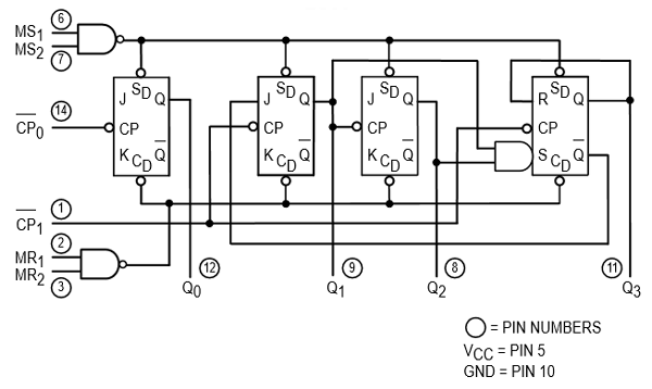
74LS90 is basically a MOD-10 decade counter that generate a BCD output code. It consists of four master-slave JK flip-flop, which are internally connected to provide MOD-2 (count to 2) counter and MOD-5 counter. 74LS90 also have an independent toggle JK flip-flop by CLKA and other three are driven by the CLKB.
Internal Logic Diagram
How to Use Decade Counter IC?
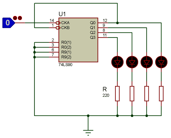
The below circuit diagram is for BCD decade counter, by giving HIGH and LOW logic to the CLKA pin, IC start counts from zero to 8 at every HIGH logic. If you want to display the number on a 7-segment display you need a seven segment display driver IC.
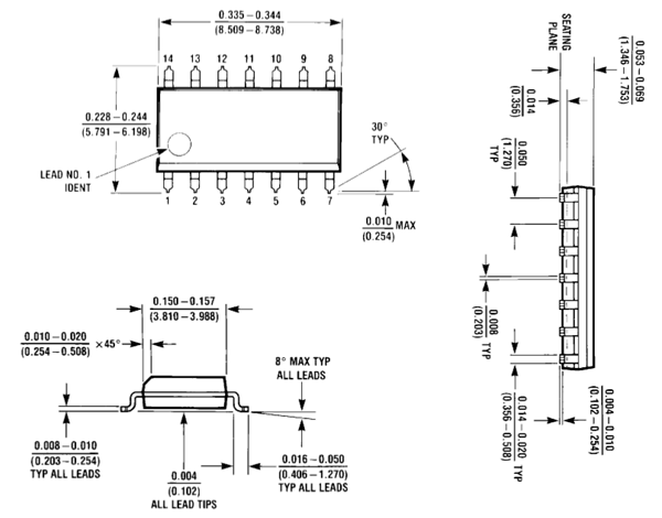
2D-model and Dimensions