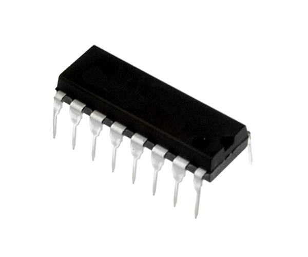
74LS83 4-bit Full Adder IC
The 74LS83 is a high speed 4-bit fuller Adder IC with carry out feature. The IC has four independent stages of full adder circuits in a single package. It is commonly used in applications where arithmetic operations are involved.
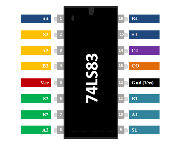
74LS83 Pin Configuration
|
Pin Number |
Pin Name |
Description |
|
10,8,3,1 |
A1, A2, A3, A4 |
First Input for the adder circuit (Four pin for four stages) |
|
11,7,4,16 |
B1, B2, B3, B4 |
Second Input for the adder circuit (Four pin for four stages) |
|
13 |
C0 |
Carry Input - from previous stage if present. |
|
9,6,2,15 |
S1, S2, S3, S4 |
Output pin for the Adder circuit (Four pin for four stages) |
|
14 |
C4 |
Carry Out pin to cascade with other ICs. |
Specifications – 74LS83
- 4-bit Full Adder with Carry Out
- Nominal Operating Voltage: 5V
- Maximum Operating Voltage: 5.5V
- Output Propagation delay: 16nS
- Maximum Input Low Voltage: 0.8V
- Minimum Input High Voltage: 2V
- Available in 16-pin PDIP, CDIP,SOIC, TSSOP packages
Note: The Specifications are applicable when the IC is operating at 5V. Complete Technical Details can be found at the 74LS83 datasheet given at the end of this page.
74LS83 Equivalents
CD4008, NTE4008
Where to use 74LS83 IC
Although today we have cheap microcontrollers that could perform all arithmetic operations required for our application, in early days the ICs like Adder, Counter, flip-flops etc were used for same. This way the complexity and the BOM cost of the circuit design will greatly go low.
The 74LS83 is a Full Adder with Carry in and Carry out feature. It is a four stage 4-bit counter, meaning it has four individual Full adder circuits each of 4-bit inside a single package. It can also be easily cascaded if more than four stages are required.
How to use a 74HC83 Full Adder IC
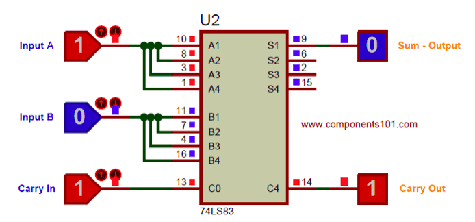
Using the Full Adder IC is pretty much straight forward. The IC has four different stages and each stage has two normal inputs Ax and Bx with an additional carry input called C1. Based on the values provided to these pins the output Sx will either be high (logic 1) or low (logic 0). The IC also has a Carry Out (CO) pin which will go high if the result has an carry. The block diagram below represents the same.
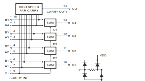
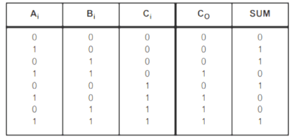
Each Full adder stage will obey the truth table below. Where Ai, Bi and Ci are the input and SUM, Co are the outputs.
Let’s understand a bit more about this IC by using a simulation. The below image and video shows the IC being simulated for all four stages by clubbing in the four input pins of both A and B. This way we can verify the truth table.
The complete working will full simulation video can be found in the video linked below.
Applications
- High Speed Arithmetic operations
- Miniature calculators
- Counters
- Simple logic control designs
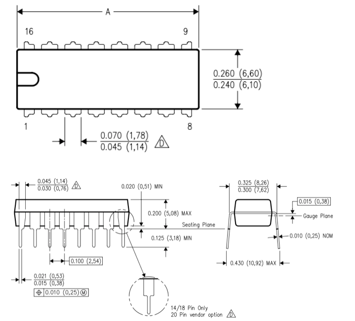
2D Model of 74LS83 (PDIP)