74LS138 – 3 to 8 Line Decoder IC
74LS138 is a member from ‘74xx’family of TTL logic gates. The chip is designed for decoding or de-multiplexing applications and comes with 3 inputs to 8 output setup. The design is also made for the chip to be used in high-performance memory-decoding or data-routing applications, requiring very short propagation delay times. In high performance memory systems these decoders can be used to minimize the effects of system decoding. The three enable pins of chip (in which Two active-low and one active-high) reduce the need for external gates or inverters when expanding. A 24-line decoder can be implemented with no external inverters, and a 32-line decoder requires only one inverter.
74LS138 is used in de-multiplexing applications by using enable pin as data input pin. Also the chip inputs are clamped with high-performance Schottky diodes to suppress line-ringing and simplify system design.
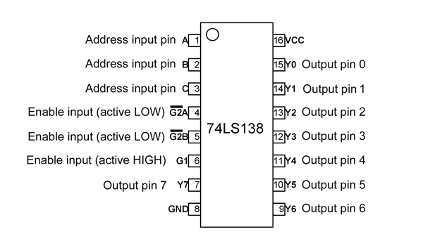
74LS138 Pin configuration
74LS138 is a sixteen pin device as shown in pin diagram and we will describe the function of each pin below.
|
Pin |
Name |
Description |
|
1 |
A |
Address input pin |
|
2 |
B |
Address input pin |
|
3 |
C |
Address input pin |
|
4 |
G2A |
Enable input (active LOW) |
|
5 |
G2B |
Enable input (active LOW) |
|
6 |
G1 |
Enable input (active HIGH) |
|
7 |
Y7 |
Output pin 7 |
|
8 |
GND |
Ground |
|
9 |
Y6 |
Output pin 6 |
|
10 |
Y5 |
Output pin 5 |
|
11 |
Y4 |
Output pin 4 |
|
12 |
Y3 |
Output pin 3 |
|
13 |
Y2 |
Output pin 2 |
|
14 |
Y1 |
Output pin 1 |
|
15 |
Y0 |
Output pin 0 |
|
16 |
VCC |
Power supply pin |
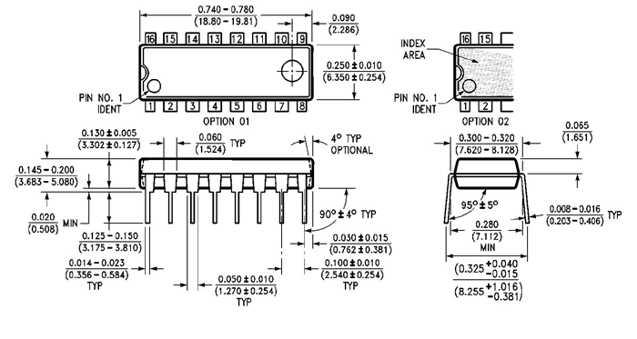
The device is available in different packages for the user to choose from.
Features and Electrical characteristics of 74LS138 Decoder
- Designed specifically for high speed
- Incorporates three enable pins to simplify cascading
- De-multiplexing capability
- Schottky clamped for high performance
- ESD protection
- Balanced propagation delays
- Inputs accept voltages higher than VCC
- Supply voltage: 1.0V to 5.5V
- Typical propagation delay: 21nS
- Low power consumption: 32mW
- Operating temperature: -40ºC to +125ºC
Similar to 74LS138 Decoder
74LS139, 74LS238 and HT12D
Overview of 74LS138 Decoder
As mentioned earlier the chip is specifically designed to be used in high-performance memory-decoding or data-routing applications which require very short propagation delay times. The memory unit data exchange rate determines the performance of any application and the delays of any kind are not tolerable there. In such applications using 74LS138 line decoder is ideal because the delay times of this device are less than the typical access time of the memory. This means that the effective system delay introduced by the decoder is negligible to affect the performance.
How to use 74LS138 Decoder
For understanding the working of device let us construct a simple application circuit with a few external components as shown below.
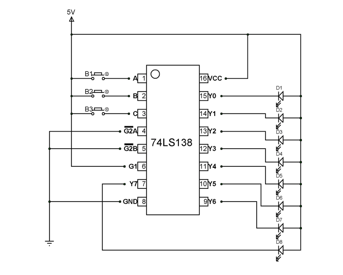
About circuit: Here the outputs are connected to LED to show which output pin goes LOW and do remember the outputs of the device are inverted. We are using a single device so we will connect G2A and G2B pin to ground followed by connecting G1 to VCC to enable the chip. The three buttons here represent three input lines for the device.
For understanding the working let us consider the truth table of the device.
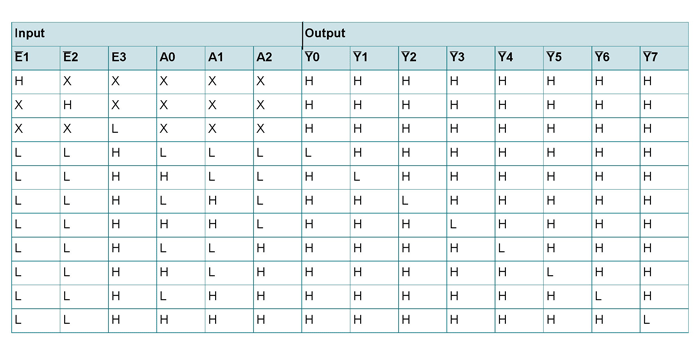
H = HIGH, L = LOW and X = Don’t Care
Working of circuit
As shown in table first three rows the enable pins needed to be connected appropriately or irrespective of input lines all outputs will be high. After connecting the enable pins as shown in circuit diagram you can use the input line to get the output.
After powering, if all buttons are not pressed Y0 will be LOW and remaining output will be HIGH as shown in table. After only B1 is pressed, A0=HIGH and Y1 will become LOW while remaining will be HIGH. Following if only B2 is pressed, A1=HIGH and Y2 will become LOW while remaining will be HIGH. This way we can realize all the truth table by toggling the three buttons B1, B2 and B3 (Three inputs A0, A1 and A2) and with that we have three input to eight output decoder.
Applications
- Line decoders
- Servers
- Digital systems
- Line De-multiplexing
- Telecom circuits
- Memory circuits
2D-Model
All dimensions are in inches (millimeter)