74HC244 Octal Buffer/Line Driver IC
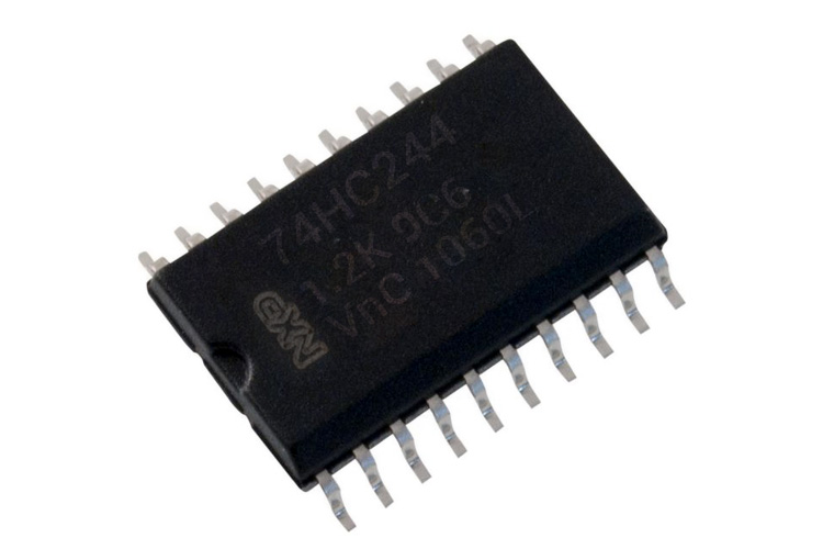
The 74HC244 IC is an 8-bit buffer or line driver IC having 3 state outputs. The IC can either be used as two 4 bit buffers or just one 8-bit buffer. The IC has a wide range of input voltage and has a very less current consumption.
Features and Specifications
This section mentions some of the important features and specifications of the 74HC244 IC.
- Supply Voltage: 2-6V DC
- Current Consumption: 80uA(Max)
- ±6-mA Output Drive at 5 V
- Inputs Level: CMOS level
- Octal bus interface
- Operating Temperatures: -40 °C to +85 °C and -40 °C to +125 °C
- Non-inverting 3-state outputs
Note: More technical information can be found in the 74HC244 Datasheet, linked at the bottom of this page.
74HC244 Pinout Configuration
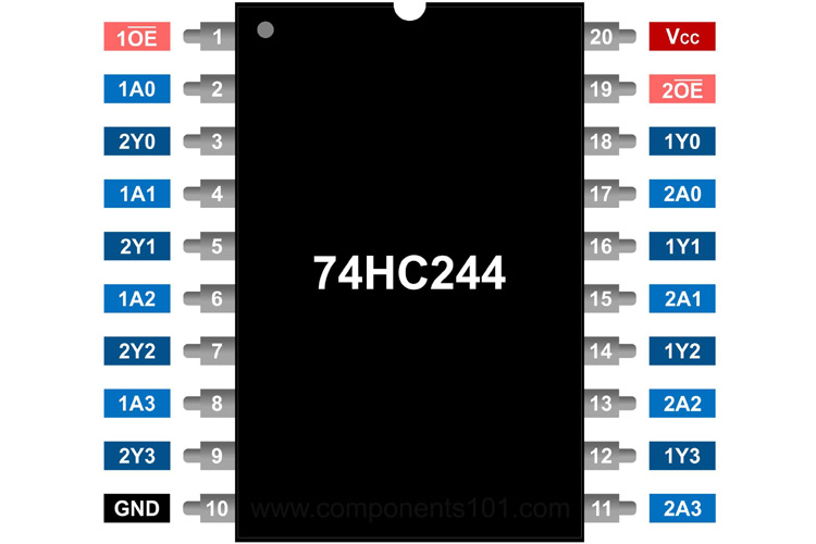
The Octal buffer IC has 20 pins for its operation and power. The table below can be referred to understand the pin configuration of the IC.
|
Pin Number |
Pin Type |
Pin Description |
|
1 |
1OE’ |
Output Enable Input(active low) |
|
2 |
1A0 |
Data Input |
|
3 |
2Y0 |
Bus Output |
|
4 |
1A1 |
Data Input |
|
5 |
2Y1 |
Bus Output |
|
6 |
1A2 |
Data Input |
|
7 |
2Y2 |
Bus Output |
|
8 |
1A3 |
Data Input |
|
9 |
2Y3 |
Bus Output |
|
10 |
GND |
Ground |
|
11 |
2A3 |
Data Input |
|
12 |
1Y3 |
Bus Output |
|
13 |
2A2 |
Data Input |
|
14 |
1Y2 |
Bus Output |
|
15 |
2A1 |
Data Input |
|
16 |
1Y1 |
Bus Output |
|
17 |
2A0 |
Data Input |
|
18 |
1Y0 |
Bus Output |
|
19 |
2OE’ |
Output Enable Input(active low) |
|
20 |
VCC |
Positive supply voltage |
Working Principle and Functional Diagram of the Octal buffer/Line Driver IC
The octal buffer IC is pretty easy to work with. The 74HC244 are organized as two 4-bit buffers with different output enable inputs.
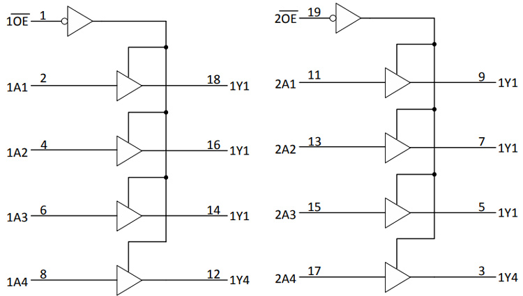
The image above shows the functional block diagram of the 74HC244 Octal buffer IC. When the Output Enable(OE’) pin 1 or pin 19 is LOW, the IC passes the non-inverted data from the Input A to the Outputs Y. Whereas, when the Output Enable(OE’) is HIGH, the Y outputs are in the high-impedance state.
Below is the truth table with different input parameters to obtain different outputs. As mentioned in the above paragraph, the state of the output enables pins to decide the output at pins Y.

Note: To make sure of the high-impedance state of the OE pin during power up and the power down of the IC, the OE pin should be hooked to the VCC pin using a pull-up resistor.
Alternatives
74HC240, 74HC541
Available Packages
SSOP, SOIC, PDIP, SOP, TSSOP
Applications
Here are some of the applications of the Octal Buffer IC.
- Motor Drivers
- LED Displays
- Servers and Telecom infrastructure
2D Model and Dimensions
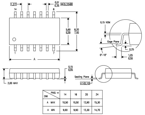
Below is the 2D model of the octal buffer IC along with its dimensions in millimeters and inches. The following information can be used in order to create custom footprints that can be used for PCB designing and CAD modelling.
